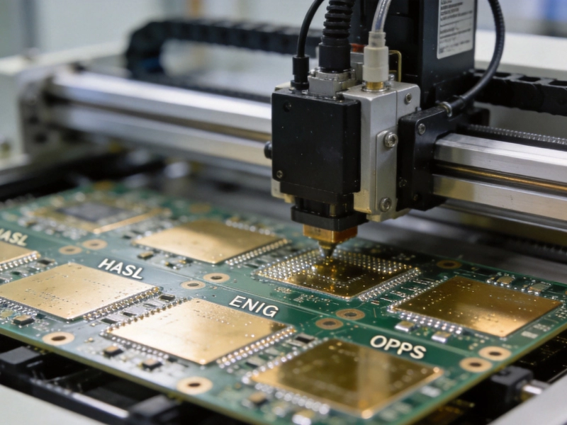
Consumer Electronics is one of the most demanding sectors for printed circuit board assembly (PCBA). Products like wearables, TWS earbuds, smart home devices, and portable audio equipment combine extreme Miniaturization, high-volume production, aggressive cost targets, and uncompromising quality expectations. For companies sourcing from China — the world's dominant Electronics Manufacturing hub — a turnkey Smt Assembly project involves far more than simply sending Gerber Files to a factory and waiting for finished boards.
This article walks through a complete turnkey SMT PCBA project in China, from initial engineering review through mass production and shipment, highlighting the critical decisions, common pitfalls, and best practices at each stage.
What "Turnkey" Really Means
In a turnkey Smt Assembly arrangement, the Contract Manufacturer (CM) handles the entire supply chain:
- PCB Fabrication — bare board manufacturing, including impedance control, surface finish, and testing
- Component Procurement — sourcing all components from authorized distributors or approved suppliers
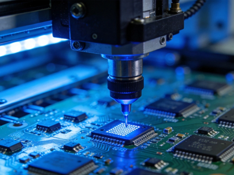
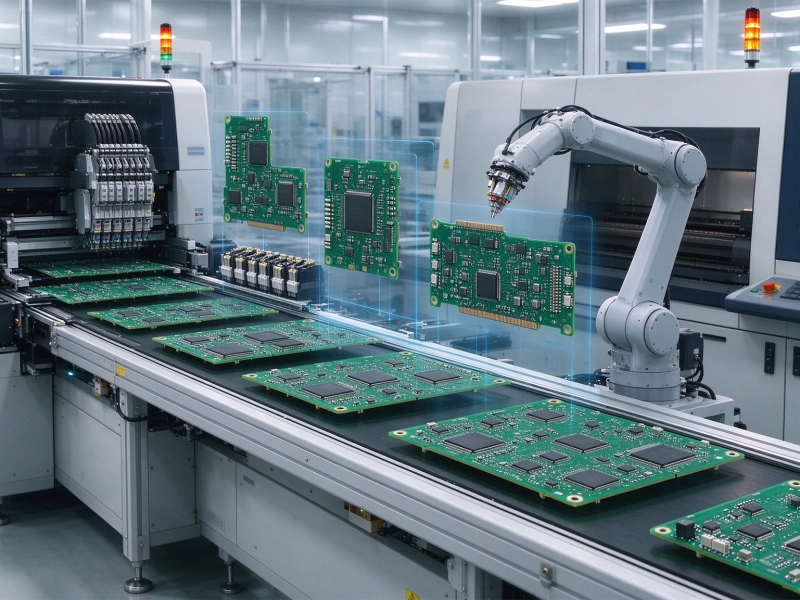
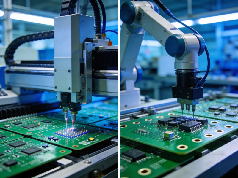
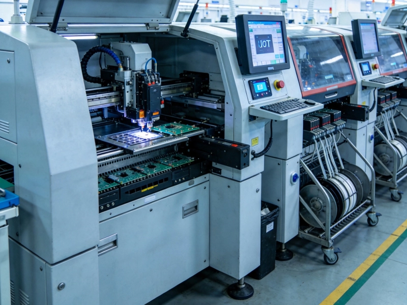
- SMT assembly — Solder Paste Printing, Component Placement, Reflow Soldering, and inspection
- Through-hole Assembly (if applicable) — Wave Soldering or selective soldering for non-SMT components
- Testing — in-circuit test (ICT), functional test (FCT), burn-in, or custom test fixtures
- Box-build and packaging — final assembly into enclosures, labeling, and packing for shipment
The alternative is a "consignment" or "Partial Turnkey" model, where the customer supplies some or all components. Turnkey shifts procurement risk and logistics burden to the CM but requires strong supply chain transparency.
Phase 1: Pre-Project Engineering Review (DFM/DFA)
Before a single component is ordered, a thorough design-for-manufacturability (Dfm) and design-for-assembly (DFA) review is essential. This is where many projects succeed or fail.
PCB Design Review
A competent CM will review your Gerber Files and provide a Dfm report covering:
- Minimum trace/space — ensuring your design matches the fabricator's capabilities (e.g., 3.5/3.5 mil for HDI)
- Via-in-pad — whether vias under BGA or fine-pitch QFN pads need to be filled and plated over
- Solder mask dams — verifying sufficient space between pads to prevent solder bridging
- Panelization — optimizing board layout within a panel for efficient SMT processing, including Fiducial Marks, tooling holes, and breakaway tabs
- Impedance control — confirming that Controlled Impedance traces have appropriate trace widths and dielectric spacing per the stack-up
Component Selection Review
For Consumer Electronics, component availability can make or break a project. Key considerations:
- Alternate parts — identifying pin-to-pin compatible alternatives for critical components (especially MLCCs, resistors, and PMICs) to mitigate shortages
- Package standardization — reducing the number of unique package sizes (e.g., consolidating 0402, 0603, and 0805 resistors where possible) to minimize feeder changes on the SMT line
- End-of-life (EOL) checks — flagging components approaching obsolescence before committing to tooling
- Counterfeit risk — ensuring all ICs and semiconductors are sourced from authorized distributors (Arrow, Avnet, Digi-Key, Mouser, etc.) rather than open markets
BOM Optimization
A well-optimized bill of materials (Bom) can reduce assembly cost by 10–20%. Common optimizations include:
- Consolidating resistor/capacitor values where circuit performance allows
- Specifying preferred manufacturers for commodity passives to leverage CM purchasing volume
- Identifying long-lead-time components early so procurement can begin before PCB Fabrication is complete
Phase 2: Prototyping and NPI
New product introduction (Npi) bridges the gap between design and mass production. A typical Npi workflow for a consumer electronics project in China follows these steps:
Step 1: Engineering Samples (5–10 units)
The first build is purely functional — verifying that the design works as intended. At this stage:
- PCBs are often fabricated using quick-turn processes (3–5 days)
- Components may be hand-sourced or pulled from distributor stock
- Assembly may involve manual placement for very low volumes
- X-ray Inspection is critical for BGA and QFN joints
Step 2: Design Validation Test (DVT) — 50–200 units
DVT units are built using production-intent processes and materials. This phase validates:
- Thermal performance under real-world operating conditions
- RF performance (for wireless devices) with production PCB materials
- Mechanical fit within the enclosure
- Compliance with relevant standards (FCC, CE, SRRC for China domestic sales)
Step 3: Production Validation Test (PVT) — 500–2,000 units
PVT is the dress rehearsal for mass production. The CM runs boards through the full SMT line at production speed, using production fixtures and test procedures. Yield data from PVT determines whether the process is ready for ramp.
Phase 3: SMT Process Details
Understanding the SMT process helps you ask the right questions and interpret quality data.
Solder Paste Printing
Solder Paste Printing is responsible for approximately 60–70% of SMT defects. Key parameters:
- Stencil design — laser-cut stainless steel stencils with electro-polished apertures; area ratio should exceed 0.66 for reliable release
- Solder paste type — Type 4 (20–38 µm particle size) is standard for fine-pitch components; Type 5 may be needed for 0.3 mm pitch BGAs or 0201 Components
- Squeegee pressure and speed — optimized through DOE (design of experiments) during NPI
- SPI (solder paste inspection) — 3D optical inspection measuring paste volume, height, and area; Cpk ≥ 1.33 is a common target
Component Placement
Modern SMT lines use a combination of high-speed chip shooters and flexible placement machines:
- Chip shooters — place passive components (resistors, capacitors) at rates exceeding 50,000 CPH (components per hour)
- Flexible placers — handle ICs, BGAs, connectors, and odd-form components with placement accuracy of ±25 µm or better
- Feeder setup — minimizing feeder changes between product runs improves efficiency; this is where Bom optimization pays off
Reflow Soldering
Reflow Profile optimization is critical for yield. A typical lead-free profile (SAC305 alloy) includes:
- Preheat — ramp at 1–3°C/second to 150–180°C
- Soak — 60–90 seconds at 150–200°C to activate flux and equalize temperatures
- Reflow — peak temperature of 240–250°C, with time above 217°C (liquidus) of 45–90 seconds
- Cooling — controlled cooling at 2–4°C/second to form proper intermetallic compounds
For consumer electronics with mixed technology (fine-pitch BGAs alongside large thermal masses like connectors), profile optimization requires careful thermocouple profiling across the board.
Inspection and Testing
A robust inspection strategy for consumer electronics includes:
- Aoi (Automated Optical Inspection) — post-reflow inspection for missing components, tombstoning, bridging, and insufficient solder
- X-ray Inspection — mandatory for BGA, QFN, and any hidden solder joints; checking for voids (typically <25% void area per Ipc-a-610 Class 2)
- ICT (in-circuit test) — verifies component values, shorts, and opens; requires a custom fixture ($2,000–$10,000 depending on complexity)
- FCT (functional test) — powers up the board and validates functionality; may include RF calibration, audio testing, or sensor calibration for wearables
- Burn-in — elevated temperature aging (e.g., 40–50°C for 24–48 hours) to screen infant mortality failures
Phase 4: Supply Chain and Logistics
China's electronics supply chain is a major advantage, but it requires active management.
Component Sourcing Strategy
- Authorized distributors — for ICs and semiconductors, insist on Traceability to authorized channels. Request certificates of conformity (CoC) for critical components.
- Local sourcing — for passives, connectors, and mechanical parts, Chinese suppliers (e.g., Fenghua Advanced Tech for resistors, Shengyi Technology for laminates) offer competitive pricing with shorter lead times.
- Safety stock — maintain 8–12 weeks of safety stock for long-lead or single-source components.
- Second sourcing — qualify alternate manufacturers for critical components during NPI to avoid supply disruptions.
PCB Fabrication Lead Times
Typical lead times from Chinese PCB fabricators:
- Quick-turn prototype — 24–72 hours for simple boards; 5–7 days for HDI or high-layer-count boards
- Standard production — 7–12 days for multilayer boards (4–8 layers)
- HDI or specialty boards — 12–20 days for any-layer HDI, heavy copper, or RF/microwave materials
Shipping and Customs
For finished goods shipment from China:
- Express (DHL/FedEx/UPS) — 3–5 days door-to-door; suitable for prototypes and small batches
- Air freight — 5–7 days; cost-effective for 100–500 kg shipments
- Sea freight — 25–35 days; the standard for mass production volumes
- Incoterms — clarify whether pricing is EXW, FOB, or DDP; FOB Shenzhen is most common for PCBA projects
Phase 5: Quality Management
Quality systems distinguish professional CMs from low-cost workshops. Key certifications and practices:
Certifications to Look For
- ISO 9001 — quality management system (baseline requirement)
- ISO 14001 — environmental management
- Iatf 16949 — Automotive Quality standard (if your consumer electronics may extend into automotive)
- Ipc-a-610 Class 2 — the standard workmanship criterion for consumer electronics; Class 3 is required for aerospace/medical
- ESD S20.20 — electrostatic discharge control program
In-Process Quality Controls
- First Article Inspection (FAI) — full verification of the first board off the line against the BOM and assembly drawings
- SPC (statistical process control) — monitoring key process parameters (paste volume, placement accuracy, reflow temperature) with control charts
- Yield tracking — monitoring first-pass yield (FPY) and defect rates by category; FPY above 98% is a reasonable target for mature consumer electronics products
- RMA analysis — root cause analysis for any field returns, with corrective action reports (8D format)
Cost Structure Breakdown
Understanding the cost drivers helps you negotiate effectively and identify optimization opportunities. A typical turnkey PCBA cost breakdown for a consumer electronics product at 10,000-unit volume:
| Cost Component | Typical Percentage | Optimization Levers |
|---|
| Components (BOM) | 50–70% | Alternate sourcing, volume pricing, value engineering |
| PCB fabrication | 10–15% | Panelization efficiency, layer count optimization, standard materials |
| SMT assembly labor | 10–15% | Design simplification, reduced unique placements, test optimization |
| Testing and programming | 5–10% | Fixture reuse, parallel testing, test time reduction |
| Overhead and profit | 10–15% | Long-term partnership, volume commitments |
Common Pitfalls and How to Avoid Them
Pitfall 1: Insufficient NPI Time
Rushing from prototype to mass production without adequate DVT/PVT phases leads to field failures. Budget 8–12 weeks for NPI on a moderately complex consumer electronics product.
Pitfall 2: Poor Communication
Time zone differences and language barriers can cause misunderstandings. Best practices:
- Assign a dedicated project manager on both sides
- Use shared documentation platforms (e.g., Agile PLM, Arena, or even structured Google Drive folders)
- Hold weekly video calls during NPI, with clear action item tracking
- Provide assembly drawings with explicit callouts for critical features
Pitfall 3: Ignoring Test Coverage
Skipping ICT or FCT to save NRE costs often results in higher field failure rates. Invest in proper test fixtures — the cost is amortized over production volume and pays for itself in reduced RMA.
Pitfall 4: Single-Source Components
A single unavailable IC can halt an entire production line. During BOM review, identify all single-source components and develop alternates or safety stock plans before PVT.
Pitfall 5: Underestimating Enclosure Integration
PCBA doesn't exist in isolation. Ensure your CM can support box-build assembly or has qualified partners for enclosure molding, final assembly, and packaging.
Selecting the Right China PCBA Partner
Not all Chinese CMs are equal. Evaluation criteria:
- Technical capability — can they handle your finest pitch component? Do they have X-ray, 3D SPI, and Aoi?
- Volume fit — some factories specialize in High-mix Low-volume (Hmlv); others excel at high-volume low-mix. Choose accordingly.
- Supply chain strength — do they have established relationships with authorized distributors? Can they provide component Traceability?
- English communication — is there a dedicated English-speaking project engineer?
- References — ask for case studies in similar product categories (wearables, audio, IoT, etc.)
- Factory audit — if volumes justify it, conduct an on-site audit or hire a third-party inspection company (e.g., QIMA, V-Trust)
Conclusion
A turnkey SMT PCBA project in China for consumer electronics is a complex undertaking that spans engineering, procurement, manufacturing, quality, and logistics. Success depends on thorough upfront DFM/DFA review, a disciplined NPI process, transparent Supply Chain Management, and a CM partnership built on clear communication and mutual accountability.
Companies that invest in these foundations consistently achieve higher yields, faster Time-to-market, and lower total cost of ownership — turning China's manufacturing ecosystem from a cost arbitrage opportunity into a genuine competitive advantage.