
Surface finish selection stands among the most consequential decisions in Pcb Design, yet its importance often receives insufficient attention until soldering problems emerge during assembly. For electronics manufacturers sourcing from China, understanding how surface finish choices affect Smt Assembly Quality proves particularly critical. Manufacturing practices, equipment capabilities, and process parameters at Chinese assembly facilities interact with surface finish characteristics in ways that differ from other manufacturing regions. Making informed surface finish decisions requires understanding these interactions and their implications for solder joint reliability.
The surface finish serves multiple essential functions: it protects copper traces from oxidation during storage and handling, it provides a solderable surface that enables reliable interconnections during assembly, and it affects the final solder joint properties that determine product reliability. Each surface finish option offers distinct advantages and limitations that must be evaluated in context of specific application requirements, assembly processes, and manufacturing partner capabilities.
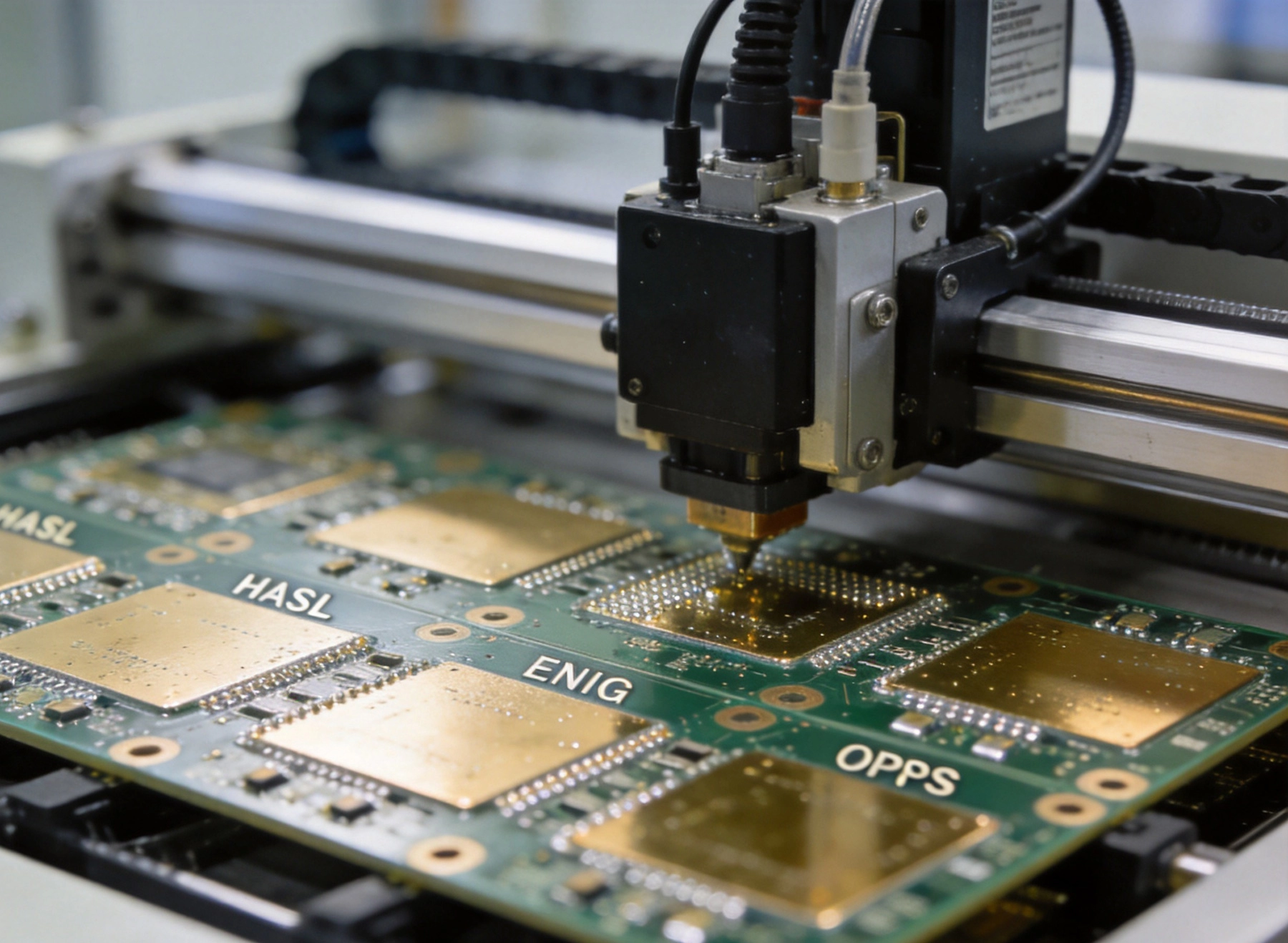
Surface finish technology has evolved significantly over decades of Electronics Manufacturing, with each generation of finishes addressing limitations identified in previous approaches. Understanding the fundamental characteristics of each finish type provides the foundation for informed selection.
HASL represents the traditional surface finish approach, applying molten solder to exposed copper surfaces before leveling with hot air knives. This process creates a characteristic uneven surface topography that has generated both advocates and critics within the industry. The HASL process deposits typically 1-25 microns of solder alloy, most commonly tin-lead or lead-free compositions.
The primary advantages of HASL include its long history of proven reliability, relatively low cost, and excellent solderability that accommodates storage periods exceeding six months under appropriate conditions. The thick solder layer provides substantial copper protection and creates robust solder joints with generous thermal cycling margins. For through-hole applications and boards with larger pad geometries, HASL remains an excellent choice.
However, HASL presents challenges for fine-pitch components. The uneven surface topography—characterized by height variations across pads and along traces—can cause alignment problems for components with pitch below 0.5mm. Thermal shock during HASL processing can damage sensitive components or laminates, though process improvements have reduced these risks. Lead-free HASL variants, required for RoHS compliance in many applications, present additional challenges due to higher processing temperatures and different solder alloy properties.
ENIG has become the dominant surface finish for fine-pitch SMT applications, particularly those requiring reliable BGA and CSP assembly. The process deposits a nickel layer (typically 3-6 microns) over copper, topped with a thin gold flash (0.05-0.2 microns) that protects the nickel from oxidation. This layered structure provides excellent shelf life and a perfectly flat surface ideal for fine-pitch components.
The flatness advantage of ENIG proves critical for area array packages like BGAs and QFNs, where coplanarity requirements demand surfaces without significant topography variation. The nickel layer provides an excellent diffusion barrier that maintains solderability even after extended storage. Gold does not diffuse into solder during reflow, instead dissolving completely to expose underlying nickel for reliable intermetallic formation.
ENIG carries notable disadvantages that limit its suitability for certain applications. The process cost substantially exceeds HASL, typically two to four times depending on board complexity and supplier. The thin gold layer can be damaged by rough handling, creating oxidation risks. Perhaps most significantly, ENIG is susceptible to "black pad" failure—a condition where improper process control creates nickel oxidation that prevents reliable solder wetting. This failure mode has caused field reliability problems in some applications.
OSP represents an environmentally friendly approach to surface preservation, applying a thin organic coating that protects copper surfaces from oxidation while maintaining solderability. The typical coating thickness of 0.2-0.5 microns allows solder to penetrate easily during reflow, creating reliable joints without the expense of precious metal finishes.
OSP offers compelling advantages including low cost, excellent flatness, and environmental acceptability without heavy metals. Multiple OSP variants exist, from simple benzotriazole-based formulations to more sophisticated imidazole derivatives that offer improved thermal resistance and extended shelf life. Selection of appropriate OSP type must consider assembly process thermal profiles and expected storage conditions.
OSP limitations include relatively short shelf life compared to ENIG or HASL, typically three to six months depending on storage conditions. The organic coating is susceptible to deterioration from humidity and temperature exposure, requiring controlled storage environments. Multiple thermal exposures—common in mixed-technology assemblies requiring selective soldering—can deplete the OSP coating, creating solderability problems on later-processed areas.
Sourcing Smt Assembly from China introduces specific considerations that influence optimal surface finish selection. Understanding how Chinese manufacturing practices interact with surface finish characteristics helps ensure appropriate decisions.
Surface finish quality at Chinese manufacturing facilities varies substantially between suppliers, reflecting differences in equipment investment, process control expertise, and quality management maturity. While major manufacturers often maintain capabilities comparable to global best practices, smaller facilities may struggle with process consistency that affects finish quality regardless of which type is selected.
For ENIG finishes, the critical "black pad" failure mode becomes more prevalent when process control lapses occur. Chinese facilities with mature ENIG processes invest in careful control of nickel bath chemistry, gold immersion kinetics, and post-treatment handling. Facilities lacking these capabilities may produce ENIG that appears acceptable initially but develops reliability problems over time.
OSP handling presents different challenges. The thin organic coating degrades faster under Chinese shipping and storage conditions—high humidity environments during summer months particularly accelerate coating deterioration. Assembly facilities must manage inventory carefully to ensure OSP-coated boards reach assembly before coating quality degrades below acceptable limits.
Surface finish selection must account for the extended supply chains typical of China Manufacturing. PCBs fabricated in China may undergo storage at multiple points between fabrication and assembly—in supplier warehouses, during transit to assembly facilities, and in assembly facility inventory before mounting. Each storage period consumes shelf life, particularly critical for OSP finishes.
For assemblies requiring multiple thermal profiles or selective soldering processes, OSP degradation between processing steps creates solderability failures. Chinese assembly facilities processing complex mixed-technology boards must carefully coordinate PCB arrival timing and storage conditions to ensure coating integrity throughout assembly sequences.
Surface finish costs vary significantly in China Manufacturing, with HASL remaining the most economical option, OSP offering mid-range pricing, and ENIG commanding premium costs. For high-volume production where assembly cost dominates, selecting the least expensive acceptable finish provides meaningful cost reduction. For specialized applications requiring ENIG performance, the premium may represent worthwhile investment in reliability.
Working with Chinese manufacturing partners to optimize finish selection requires transparent discussion of application requirements, storage expectations, and quality standards. Partners who understand the technical trade-offs can guide selection that balances cost against performance requirements rather than defaulting to premium options that may not be necessary.
Surface finish directly affects the properties of finished solder joints, with implications for both immediate assembly yield and long-term field reliability.
Wetting—the process by which molten solder flows and bonds to metal surfaces—proceeds differently depending on surface finish characteristics. HASL surfaces, with their thick solder coating, provide essentially immediate solderability regardless of pad surface condition. The HASL solder itself becomes part of the joint, creating characteristic microstructures that differ from joints formed on ENIG or OSP surfaces.
ENIG surfaces rely on intermetallic formation between solder and underlying nickel, a process that requires slightly longer reflow times and appropriate temperature profiles. The nickel-gold-solder system creates predictable intermetallic layers, but process deviations can create either insufficient intermetallic formation or excessive growth that embrittles joints.
OSP surfaces present unique wetting dynamics. Solder must penetrate the organic coating to reach copper beneath, requiring flux activation and appropriate thermal profiles. If OSP coating is too thick or improperly formulated, incomplete wetting creates unreliable joints. If coating is depleted before assembly, copper oxidation creates similar problems.
Thermal cycling resistance varies substantially between surface finish types. HASL joints, with their ductile solder composition and thick joint geometry, typically demonstrate excellent thermal cycling performance. The thick solder layer accommodates plastic deformation during thermal excursions without fatigue cracking.
ENIG joints face different failure mechanisms. The thin bonding layer between solder and nickel creates different stress distributions than HASL joints. While properly formed ENIG joints demonstrate excellent thermal cycling capability, process problems—particularly black pad conditions—create weak interfaces susceptible to failure under thermal stress.
OSP joint reliability depends heavily on proper flux selection and thermal profile optimization. The direct copper-solder interface provides excellent metallurgical bonding when properly formed. However, any contamination or oxidation on copper surfaces before OSP application creates defects that compromise reliability.
Portable electronics and products subject to mechanical shock require surface finishes that support robust mechanical joints. HASL joints generally perform well under mechanical stress due to their ductile nature and generous geometry. The thick solder deposits absorb shock energy without crack propagation.
ENIG joint performance under mechanical stress has generated ongoing debate. Some studies suggest ENIG joints may be more susceptible to brittle fracture under severe shock conditions, particularly when intermetallic layers are excessively thick. However, properly processed ENIG joints can achieve mechanical reliability comparable to HASL, with differences primarily reflecting process quality rather than fundamental surface finish characteristics.
Optimal surface finish selection depends on specific application requirements that must be evaluated holistically.
Assemblies incorporating BGA, CSP, QFN, or fine-pitch QFP components require surface finishes that provide coplanarity and consistent solderability. HASL surfaces with their irregular topography can create alignment problems and inconsistent paste release that compromise assembly yield for these components.
ENIG provides the flat surface and consistent solderability that fine-pitch assembly demands. The uniform coating ensures predictable paste transfer during printing and consistent wetting during reflow. For production involving BGAs with pitch below 0.8mm, ENIG has become essentially mandatory.
OSP can support fine-pitch assembly if process parameters are optimized. The flat surface supports paste printing consistency, and proper flux selection ensures complete wetting. However, the multiple heating cycles common in complex assemblies may deplete OSP coating on later-processed components.
Assemblies combining SMT components with through-hole devices present different surface finish requirements. HASL remains excellent for through-hole applications, with its thick solder layer filling holes reliably and supporting Wave Soldering processes. The uneven HASL surface topography affects only SMT pads, not through-hole functionality.
ENIG can work for through-hole applications but requires attention to hole wall coverage and plating quality. The thin nickel-gold deposit may not provide equivalent solderability in holes compared to bulk HASL deposits. Testing should verify through-hole solder fill before committing to ENIG for mixed-technology assemblies.
OSP presents challenges for through-hole applications. Wave Soldering processes may not reliably fill holes with the thin organic coating, particularly for boards with thermal mass that delays reaching solder melting temperature. Selective plating or solder fountain processes may be required to ensure adequate through-hole fill.
Automotive, medical, and aerospace applications impose stringent reliability requirements that influence surface finish selection. These applications typically specify ENIG despite its higher cost, valuing the consistent quality and proven reliability record in demanding environments.
For automotive applications, ENIG with appropriate process controls has become the dominant surface finish specification. The flat surface supports the fine-pitch components common in Automotive Electronics while providing the shelf life stability needed for complex supply chains. Iatf 16949 quality system requirements drive process discipline that mitigates black pad risks.
Medical device applications may require ENIG or alternative precious metal finishes depending on regulatory pathway and sterilization requirements. Gold finishes offer biocompatibility advantages in some applications, though cost premiums are substantial.
Achieving optimal soldering results requires surface finish-specific process optimization that Chinese assembly facilities should implement.
ENIG process control requires attention to multiple parameters that affect nickel deposit properties. Phosphorus content in the nickel layer (typically 6-10%) influences corrosion resistance and solderability. Lower phosphorus levels improve corrosion resistance but may create solderability problems. Higher phosphorus levels provide better solderability but may be more susceptible to oxidation.
Gold thickness must be carefully controlled. Too thin, and the gold cannot fully protect nickel during storage. Too thick, and gold dissolution during reflow may be incomplete, potentially creating voids or weak joints. The typical specification of 0.05-0.2 microns represents an acceptable balance that Chinese facilities should target consistently.
OSP storage and handling requires conditions that preserve coating integrity. Relative humidity should be maintained below 60% RH, with temperature controlled below 30°C. Boards should be sealed in moisture-barrier bags with appropriate desiccants. Storage duration should be tracked to ensure boards are processed within coating shelf life limits.
Assembly facilities should verify incoming OSP coating quality and reject boards showing visible oxidation or discoloration. For complex assemblies requiring multiple thermal profiles, coordination between PCB Fabrication date and assembly scheduling ensures adequate coating remaining for all processing steps.
The transition to lead-free solders, driven by RoHS requirements, has affected surface finish selection and processing. Lead-free HASL (LF-HASL) requires higher processing temperatures that create laminate stress and potentially damage sensitive components. The tin-copper and tin-silver-copper alloys used in LF-HASL also form different intermetallic compounds than traditional tin-lead solder.
ENIG and OSP processes adapt more readily to lead-free requirements, as their fundamental characteristics remain similar regardless of solder alloy. However, lead-free reflow profiles with higher peak temperatures may require adjusted ENIG processing or OSP formulation selection to maintain coating integrity throughout assembly.
Verifying surface finish quality protects against problems that could affect assembly reliability.
Visual inspection should verify finish appearance consistent with specifications—no discoloration, oxidation, or handling damage. For ENIG, the characteristic bright gold appearance should be uniform across the board. HASL surfaces should show consistent solder coverage without voids or lumps. OSP surfaces should appear uniform copper-colored without oxidation patterns.
Solubility testing provides quantitative assessment of surface condition. Wetting balance testing measures force versus time curves during immersion in solder, providing objective assessment of solderability. While more expensive than visual inspection, this method identifies subtle degradation invisible to visual examination.
Assembly facilities should monitor process indicators that signal surface finish-related problems. Solder paste release during printing, wetting behavior during reflow, and joint appearance after cooling all provide feedback on surface condition. Facilities should track defect patterns—solder opens, insufficient wetting, or cold joints—that may indicate surface finish issues.
X-ray Inspection of BGAs and other hidden joints reveals internal joint structure that may indicate surface finish problems. Voids, incomplete fill, or irregular intermetallic formation can signal process issues including surface finish degradation. Regular X-ray sampling provides early warning of emerging problems.
Surface finish selection profoundly impacts Smt Assembly Quality in China manufacturing, affecting everything from immediate assembly yield to long-term field reliability. Each finish type offers distinct characteristics that suit different applications—HASL for cost-effective through-hole and large-pad applications, ENIG for fine-pitch and high-reliability requirements, OSP for cost-sensitive applications with appropriate process control.
Successful surface finish implementation requires matching finish characteristics to manufacturing partner capabilities, supply chain logistics, and application requirements. Chinese assembly facilities with mature processes can produce excellent results across all major finish types, but process control discipline varies across the supplier landscape. Understanding this variation helps ensure appropriate partner selection and expectation management.
The optimal approach combines thorough incoming inspection with process monitoring that identifies surface finish-related problems before they affect production quality. Working collaboratively with manufacturing partners to optimize processes for specific finish types ensures that surface finish investments deliver their intended reliability benefits throughout product lifetime.
ENIG provides the flat surface, consistent solderability, and excellent shelf life that Bga Assembly demands. The uniform topography ensures coplanarity requirements are met, while the nickel-gold system creates reliable intermetallic bonding. For high-reliaibility BGAs, ENIG with tight process control minimizes black pad risks that could compromise joint reliability.
Surface finish affects yield primarily through solderability consistency and topography. Poor solderability—due to finish degradation or contamination—creates wetting failures, opens, and insufficient joints. Excessive topography—primarily with HASL—can cause alignment and paste transfer problems for fine-pitch components. Process control quality at specific facilities determines how consistently any finish type performs.
HASL typically maintains solderability for 6-12 months under proper storage conditions. ENIG provides the longest shelf life, often exceeding 12 months due to the protective gold layer. OSP has the shortest shelf life, typically 3-6 months, depending on specific formulation and storage conditions. For supply chains involving extended storage or transport, these shelf life differences affect inventory management requirements.
OSP can work for multiple thermal processes if coating thickness and formulation are appropriate and thermal profiles are optimized. However, each thermal exposure depletes the OSP coating, potentially creating solderability problems on later-processed components. For complex assemblies with selective soldering or multiple reflow profiles, ENIG typically provides more forgiving processing latitude.
Verification should combine visual inspection for obvious defects with solderability testing for objective quality assessment. Request process certifications and material certifications from suppliers. For critical applications, consider incoming inspection programs that measure solderability directly. X-ray Inspection of assembled joints provides feedback on whether surface finish processing achieved reliable results.
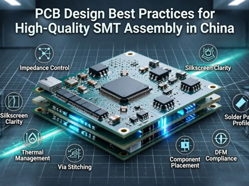
PCB Design Best Practices for High-Quality SMT Assembly in ChinaJune/05/2026
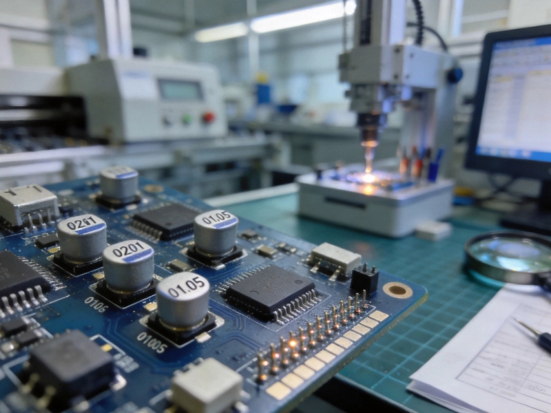
Designing for Miniaturization: 0201 and 01005 Components in China SMT AssemblyJuly/26/2026
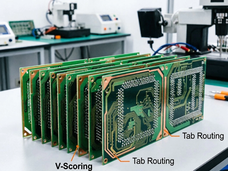
PCB Panelization Guide for SMT Assembly China: V-Scoring vs. Tab RoutingJuly/03/2026
Thermal Management in PCB Design: Preventing Warpage in China's SMT AssemblyJuly/15/2026
PCB Design Best Practices for High-Quality SMT Assembly in ChinaMay/29/2026

Avoiding Tombstoning: PCB Design Tips for Passive SMT Components in China AssemblyOctober/10/2026
How to Design the Perfect Land Pattern for SMT Components in Chinese FactoriesJune/18/2026
PCB Stack-up Considerations for Reliable SMT PCB Assembly in Chinese Supply ChainsSeptember/20/2026