Open Nav

Shenzhen, China has long been recognized as the global epicenter of Electronics Manufacturing, attracting startups, scale-ups, and Fortune 500 companies alike to its dense ecosystem of component suppliers, contract manufacturers, and specialized service providers. For companies developing custom Internet of Things (IoT) products, Shenzhen offers a unique combination of rapid prototyping capabilities, scalable production capacity, and component sourcing infrastructure that is difficult to find anywhere else in the world.
But navigating a custom IoT PCB assembly project in Shenzhen—from initial concept through to finished, shipped products—can feel overwhelming for those unfamiliar with the process. The city is vast, suppliers range from world-class facilities to small workshops, and the gap between a great prototype and a reliable production run can be wider than many first-timers expect.
This article follows a complete custom IoT Smt Pcb Assembly project from concept to reality, walking through every stage of the process, typical timelines, key decisions, and practical lessons learned along the way.
To make this discussion concrete, we follow a representative project: a startup developing a battery-powered smart environmental sensor that monitors temperature, humidity, and air quality in commercial buildings. The device uses an ESP32 module for Wi-Fi connectivity, a BME680 sensor for environmental data, a small OLED display for local status, and is designed for indoor wall mounting with a battery life of at least 2 years.
The product targets initial production of 500 units, with plans to scale to 5,000 units within 12 months. The team consists of 3 hardware engineers based in the United States, with limited prior experience working with Shenzhen manufacturers.
This project profile— a moderately complex IoT device, low-to-medium initial volume, overseas development team— is extremely common and reflects the reality facing most IoT hardware startups and product companies today.
Every successful IoT PCB project begins long before the first design file is sent to a manufacturer. In the concept stage, the team defines the product requirements, selects key components, and establishes the high-level architecture that will guide the entire development process.
The first step is to clearly define what the product needs to do, under what conditions it must operate, and what constraints exist on size, cost, power consumption, and connectivity. For the smart environmental sensor, key requirements included:
Defining these requirements clearly at the outset prevents costly redesigns later. Many first-time IoT hardware developers underestimate the importance of this stage, jumping directly to schematic capture before fully considering battery life, enclosure constraints, regulatory requirements, and cost targets.
For an IoT device destined for Shenzhen manufacturing, component selection is critically linked to sourcing. Some components that are readily available in the US may be difficult to source in Shenzhen, or may carry significant price premiums for small order quantities. Conversely, many components are much more readily available and affordable in Shenzhen due to the proximity of major component distributors and trading companies.
The team conducted a preliminary sourcing assessment, identifying the key components for the environmental sensor: ESP32-WROOM module, BME680 sensor, 0.96-inch OLED display, and a small MCU for power management. All of these components are widely available from Shenzhen-based distributors and trading companies, with lead times of 1-2 weeks for most quantities. This early sourcing verification gave the team confidence that the design could be manufactured in Shenzhen without supply chain surprises.
A critical lesson at this stage: always confirm component availability and pricing with your chosen manufacturer or a sourcing partner in Shenzhen before finalizing your component selection. A design that looks great on paper can hit a wall if a key component has a 26-week lead time or is only available in minimum quantities of 10,000 units.
With requirements and components defined, the engineering team moves into the detailed design phase. For a moderately complex IoT device like this environmental sensor, the design phase typically takes 6-8 weeks for a team working part-time on the project.
The schematic captures the electrical design: all components, their connections, power distribution, signal routing, and interface definitions. For the environmental sensor, the schematic included the ESP32 module with its antenna matching circuit, the BME680 I2C sensor interface, the OLED display driver, power management circuitry including a low-quiescent-current LDO and battery protection, and a USB-C charging circuit for an optional rechargeable battery version.
During schematic capture, the team engaged their Shenzhen manufacturer for a preliminary Dfm (Design For Manufacturability) review. This early engagement—well before the layout was finalized—allowed the manufacturer to flag potential issues with component packages, via sizes, and trace spacing that would have been difficult or expensive to change later in the design process.
Pcb Layout is where the design intent meets the realities of manufacturing. The environmental sensor uses a 4-layer PCB with the following key layout considerations:
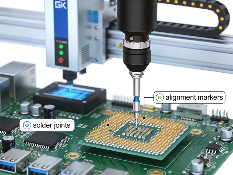
The layout was reviewed by the Shenzhen manufacturer's engineering team before final release. This review identified several improvements, including adding ground stitching vias around the antenna keep-out zone, adjusting the pad sizes for a few components to match the manufacturer's standard SMT profiles, and adding Fiducial Marks for Automated Optical Inspection alignment.
The Dfm review is one of the most valuable steps in the entire project, and it should never be skipped. The manufacturer's engineering team reviewed the complete design package—Gerbers, drill files, BOM, pick-and-place file, stackup specification, and impedance requirements—and returned a detailed report identifying:
The team addressed all of these issues before releasing the design for production, saving an estimated 3-4 weeks of potential respin delays that would have occurred if the issues had been discovered after the first prototype build.
With a DFM-cleaned design, the team moved to prototype production. Prototype builds in Shenzhen typically range from 5-20 units and are priced at a premium compared to production runs, reflecting the setup costs and lower economies of scale. For the environmental sensor, the prototype build of 15 units cost approximately $2,200 including PCB fabrication, component procurement, assembly, and basic testing.
The bare PCBs were fabricated in 5 working days by a Shenzhen Pcb Manufacturer specializing in quick-turn prototyping. The 4-layer board with Controlled Impedance cost $380 for 15 panels (each panel containing 4 individual boards), with a 2-day expedited option available for an additional $120. The manufacturer used 1.0mm thick Rogers RO4003C material for the core, with standard FR-4 prepregs for the build-up layers, achieving the impedance control required for the ESP32 RF interface.
Component procurement for the prototype run took the most time, as several components had to be sourced from distributors with 1-2 week lead times. The BME680 sensor, in particular, had a 10-day lead time from the primary distributor. The manufacturer managed the procurement process, identifying the fastest available sources and coordinating deliveries to align with the PCB fabrication timeline. Total component cost for 15 units was approximately $1,100.
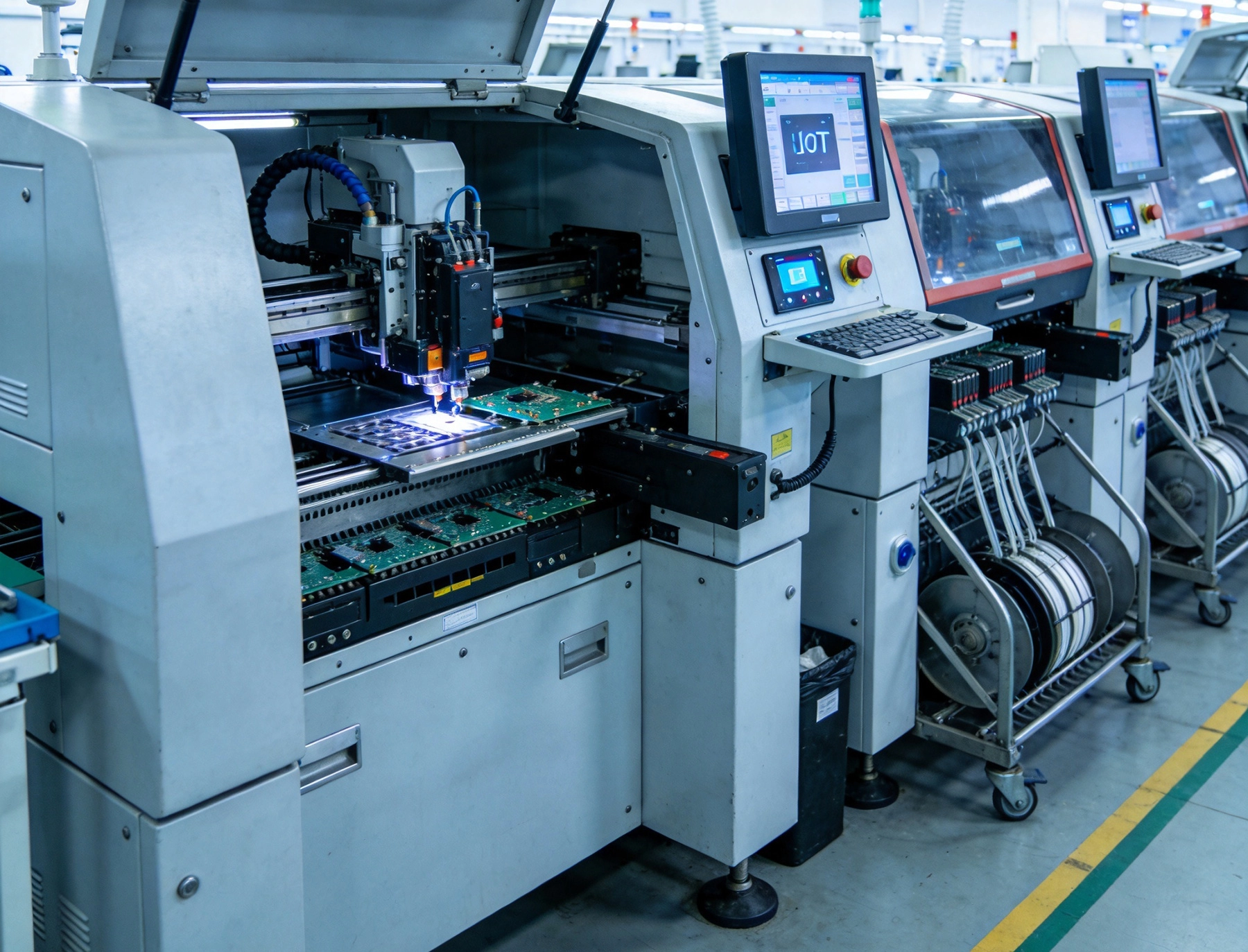
Smt Assembly was completed in 2 days. The manufacturer used a full SMT line including Solder Paste Printing, high-speed pick-and-place for passive components, fine-pitch placement for the QFN and BGA packages, Reflow Soldering, and Aoi (Automated Optical Inspection) after reflow. The ESP32-WROOM module required careful Reflow Profile optimization to ensure reliable solder joint formation without damaging the module's internal components.
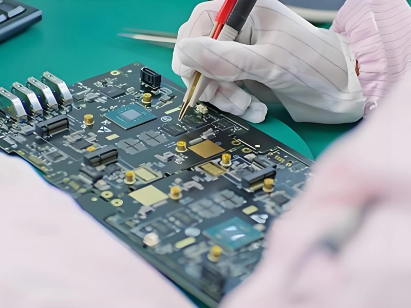
Following Smt Assembly, the board went through through-hole component insertion (the battery holder and a connector) and hand assembly (the coin cell holder and the external sensor connector). The manufacturer assigned a skilled technician to these operations, and the boards were inspected under magnification to verify solder joint quality.
The final stage of prototype build was in-circuit testing, programming, and functional validation. The manufacturer performed basic in-circuit testing to verify that all traces were properly connected and no open or short circuits existed. The team then programmed the firmware onto each ESP32 module and ran a comprehensive functional test, verifying sensor readings, display operation, Wi-Fi connectivity, MQTT data reporting, and power consumption.
Of the 15 prototype units, 14 passed all functional tests and were delivered to the team for further validation. One unit had a dry joint on the BME680 sensor that was quickly reworked. This 93% first-pass yield is typical for well-designed prototype builds and reflects the value of thorough Dfm Review before releasing the design.
The prototype units underwent 5 weeks of extensive testing and validation by the engineering team. This stage revealed several issues that needed to be addressed before proceeding to production:
Each of these issues required a design revision and a second prototype build. The manufacturer supported two additional quick-turn prototype builds of 10 units each, at a total cost of approximately $2,800. By the end of this stage, the team had a fully validated design ready for production.
A critical lesson from this stage: budget time and money for at least two prototype iterations. Even the most carefully designed IoT products invariably require at least one respin to address issues discovered during functional testing. First-time hardware developers often underestimate the time and cost of this stage, which typically takes as long as the original design phase.
With a validated design in hand, the team moved to prepare for production. This stage involves finalizing the manufacturing setup, qualifying the production process, and establishing quality procedures for the production run.
The team prepared a complete production data package for the manufacturer, including final Gerber files, updated drill files, the BOM with confirmed pricing for production quantities, the pick-and-place file with Component Placement coordinates, the stackup and impedance specification, assembly drawings with special instructions, test procedures and acceptance criteria, regulatory compliance documentation, and packaging and labeling specifications.
Before committing to the full production run, the manufacturer produced a first article of 10 units using the production process and settings planned for the volume run. These units underwent detailed inspection against the original specifications, including dimensional verification, electrical testing, functional testing, and visual inspection. Any deviations from specifications were identified and corrected before the production run proceeded.
The manufacturer conducted process qualification specific to the environmental sensor design, including solder paste height measurements for the fine-pitch QFN components, X-ray Inspection of BGA and QFN solder joints, thermal profiling of the reflow oven for the specific board mass and thermal characteristics, and pull testing of solder joints on selected components.
All process qualifications passed, and the manufacturer confirmed that the production line was ready for the volume run.
For the initial production run of 500 units, the manufacturer stocked components based on the BOM requirements plus a 5% buffer for loss and defectives. Components with longer lead times or single-source dependencies were stocked with a larger buffer of 10-15%. Total component inventory value for the production run was approximately $28,000.
The volume production run of 500 units was completed over approximately 6 weeks, including PCB fabrication, component procurement, SMT assembly, Through-hole Assembly, testing, programming, and packaging.
The 500 units required 125 panels (4 units per panel) of 4-layer PCBs. PCB fabrication took 8 working days at the manufacturer's facility. Total PCB fabrication cost for the full run was approximately $6,200 ($12.40 per unit), significantly lower than the prototype unit cost of $25 per board due to economies of scale.
Components were procured from the pre-stocked inventory, with the manufacturer procuring an additional $8,000 in components to replenish buffers for the next production run. Component cost per unit for the production run was approximately $6.80, down from approximately $73 per unit during prototyping due to volume pricing and the efficiency of consolidated procurement.
SMT assembly of all 500 units took 4 working days across two production shifts. The manufacturer achieved a first-pass yield of 97.2% (486 of 500 units passing all tests without rework), with 14 units requiring minor rework for touch-up soldering and component replacement. This yield rate is excellent for a medium-complexity IoT device and reflects the thorough preparation and DFM work done earlier in the project.
All 500 units underwent in-circuit testing, firmware programming, and functional testing. Programming was performed using a custom fixture that simultaneously programmed 8 boards, reducing programming time to approximately 45 seconds per batch of 8 units. Total test and programming time for the full run was approximately 3 days.
Each finished unit underwent final visual inspection, was paired with its enclosure hardware and battery, and was packaged in a retail-ready box with labeling, user manual, and accessories. Packaging was completed in 2 days.
Total production cost for 500 units, including PCB fabrication, components, assembly, testing, programming, and packaging, was approximately $23,000— translating to $46 per finished, packaged unit. This is well within the team's cost target and leaves healthy margins at the planned retail price point.
With all 500 units completed and tested, the final stage was logistics: getting the finished products from Shenzhen to the team's warehouse in the United States.
The manufacturer coordinated international shipping through their established logistics partner. The shipment of 500 units in 12 cartons was shipped via air freight to Los Angeles, with a total shipping cost of approximately $1,800. Customs clearance was managed by a customs broker engaged by the team, with duties and import fees of approximately $2,100 (based on the HS code classification for the product). Total logistics cost was approximately $3,900, or $7.80 per unit.
Combining production costs ($46/unit) and logistics costs ($7.80/unit), the total landed cost for the finished environmental sensor was approximately $53.80 per unit— well within the team's target of under $60 per unit including all costs.
Units arrived at the team's warehouse 10 days after shipment from Shenzhen, in excellent condition with no damage in transit. The entire project, from initial concept to delivered products, took approximately 37 weeks.
Reflecting on this project, several key lessons emerge that apply broadly to any custom IoT PCB assembly project in Shenzhen:
Custom IoT PCB assembly in Shenzhen is a powerful pathway from concept to commercial product, offering unmatched access to world-class manufacturing capabilities, component sourcing, and production capacity at competitive costs. But it is not a simple transaction—it is a collaborative process that rewards preparation, clear communication, and partnership with experienced manufacturers.
The project outlined in this article— from initial concept through delivered products in 37 weeks— is representative of what is achievable with proper planning, thorough DFM engagement, realistic budgeting for prototype iterations, and a commitment to quality at every stage. For IoT hardware developers and product companies looking to bring their designs to market, Shenzhen remains one of the most powerful manufacturing ecosystems in the world, capable of supporting projects from the earliest prototype through high-volume mass production.
The key is to approach the process with the same rigor and preparation you would apply to any complex engineering project— because that is exactly what it is.
A: For a moderately complex IoT device like the one described in this article, a realistic timeline is 6-9 months from concept to delivered products. This includes 4-6 weeks for design, 4-8 weeks for prototype builds and iterations, 2-4 weeks for production preparation, and 4-8 weeks for volume production and shipping. More complex devices with advanced packaging, regulatory certification requirements, or novel components can take significantly longer.
A: Prototype Assembly costs in Shenzhen vary widely based on complexity, but as a rough guide, expect to pay $100-300 per assembled prototype unit for a moderately complex device, including PCB fabrication, components, assembly, and basic testing. Simple 2-layer boards with mostly passives may be $50-80 per unit, while complex multi-layer or HDI boards can be $500 or more per prototype unit.
A: Several approaches work well: industry referrals from other companies with similar projects, visits to electronics trade shows where Shenzhen manufacturers exhibit, working with a sourcing agent or Contract Manufacturer with established Shenzhen relationships, and using online platforms that vet and connect with verified manufacturers. Regardless of the channel, always validate a manufacturer's capabilities with a small prototype order before committing to a larger production run.
A: The biggest risks are component supply chain disruptions, quality control failures, communication and language barriers, and intellectual property protection. Mitigate these risks by diversifying component sources where possible, requiring detailed quality procedures and inspection criteria, building strong communication channels with your manufacturer, and working with manufacturers that have established IP protection policies. A well-prepared DFM package and clear quality acceptance criteria go a long way toward preventing quality issues before they occur.
Overcoming BGA Challenges in a Complex SMT PCB Assembly China ProjectMay/29/2026

Automotive Electronics Success: High-Reliability SMT PCB Assembly China Case StudyJuly/17/2026
Overcoming BGA Challenges in a Complex SMT PCB Assembly China ProjectJune/09/2026
Solving Thermal Issues in LED SMT PCB Assembly: A Real-World China Factory ExampleJuly/28/2026
How We Helped a US Startup Scale from Prototype to Mass SMT Assembly in ChinaJuly/07/2026
Why IPC Class 3 Standards Matter for Industrial SMT PCB Assembly in ChinaJuly/08/2026
Thermal Management in PCB Design: Preventing Warpage in China's SMT AssemblyJuly/15/2026
SMT vs THT PCB Assembly in China: Which Technology is Right for Your Project?June/08/2026