Open Nav
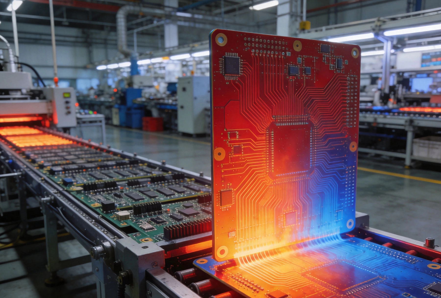
Thermal Management in PCB Design: Preventing Warpage in China's SMT AssemblyJuly/15/2026You receive your first production shipment from a contract manufacturer in Shenzhen. The boards look perfect—until you run them through reflow and watch them twist like potato chips cooling on a counter. The warpage exceeds tolerances. Components are misaligned. The entire order becomes scrap....
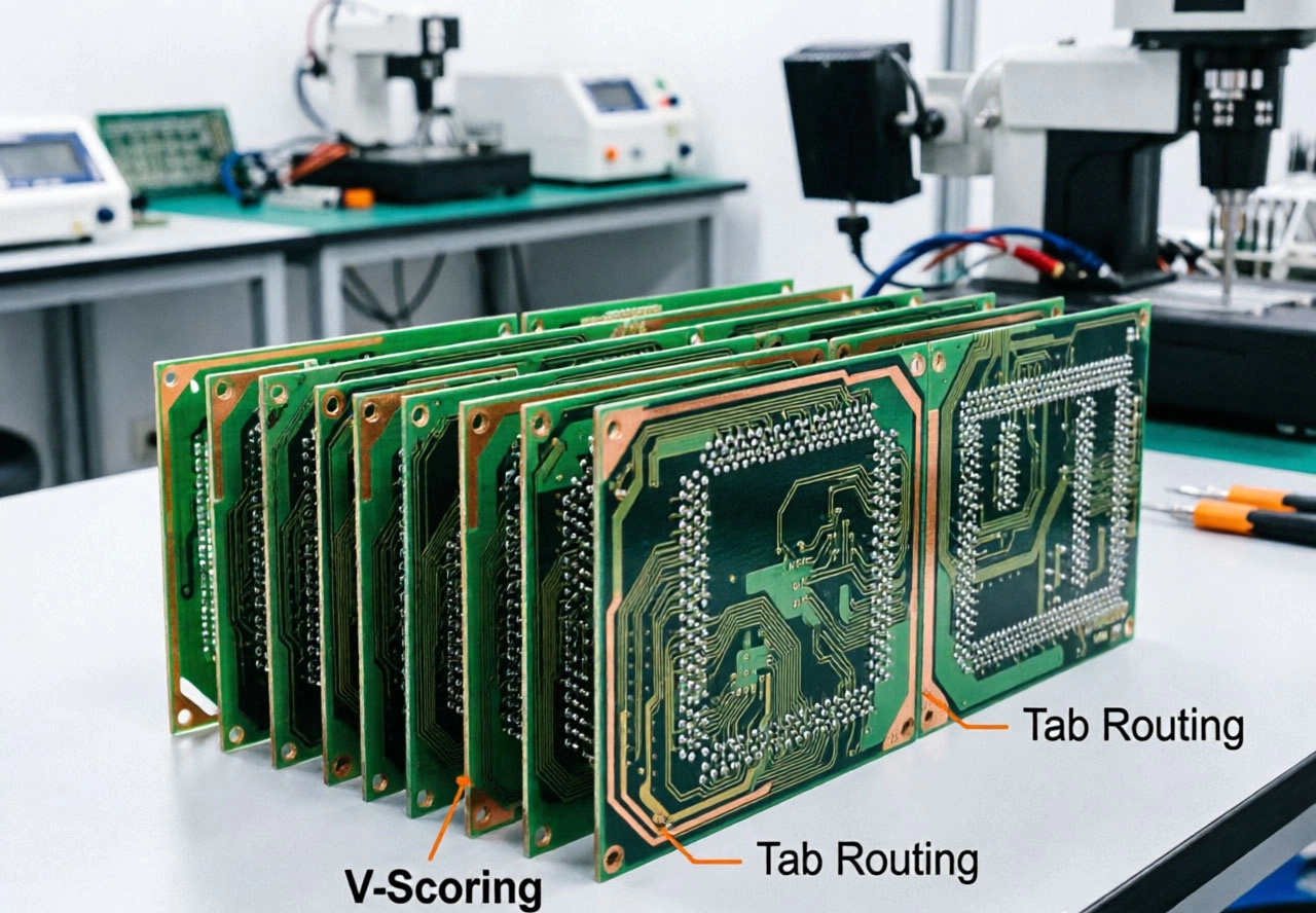
PCB Panelization Guide for SMT Assembly China: V-Scoring vs. Tab RoutingJuly/03/2026China's electronics manufacturing industry has matured into the world's most capable and cost-effective production ecosystem, with thousands of SMT assembly facilities serving global brands from consumer electronics to aerospace components. At the heart of efficient SMT production lies a critical ...
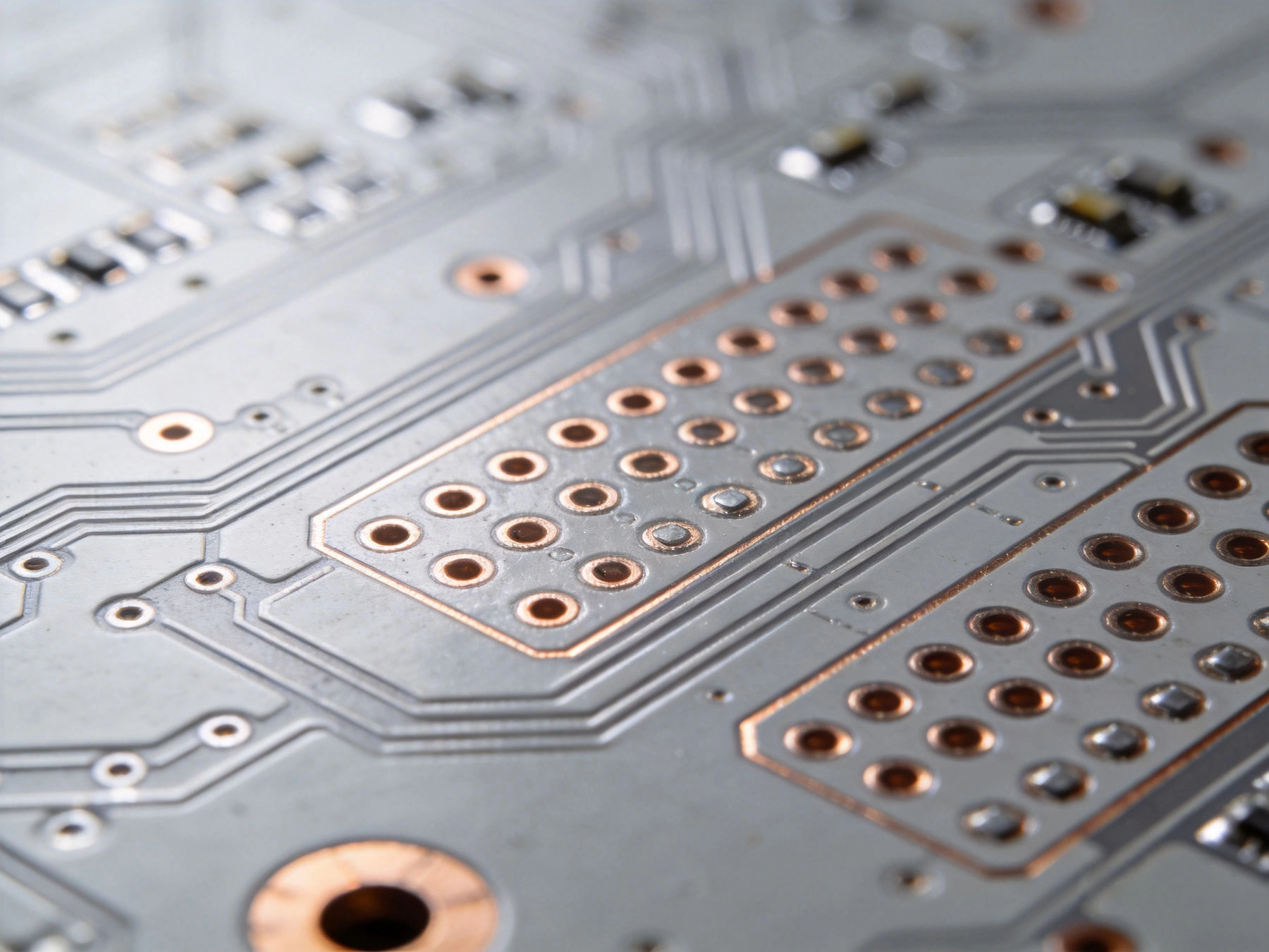
How to Design the Perfect Land Pattern for SMT Components in Chinese FactoriesJune/18/2026When you partner with electronics manufacturers in China, getting your land pattern designs right isn't just a technical detail—it's the difference between smooth production runs and costly respins. Your PCB footprint directly impacts solder joint reliability, assembly yield rates, and long-term p...
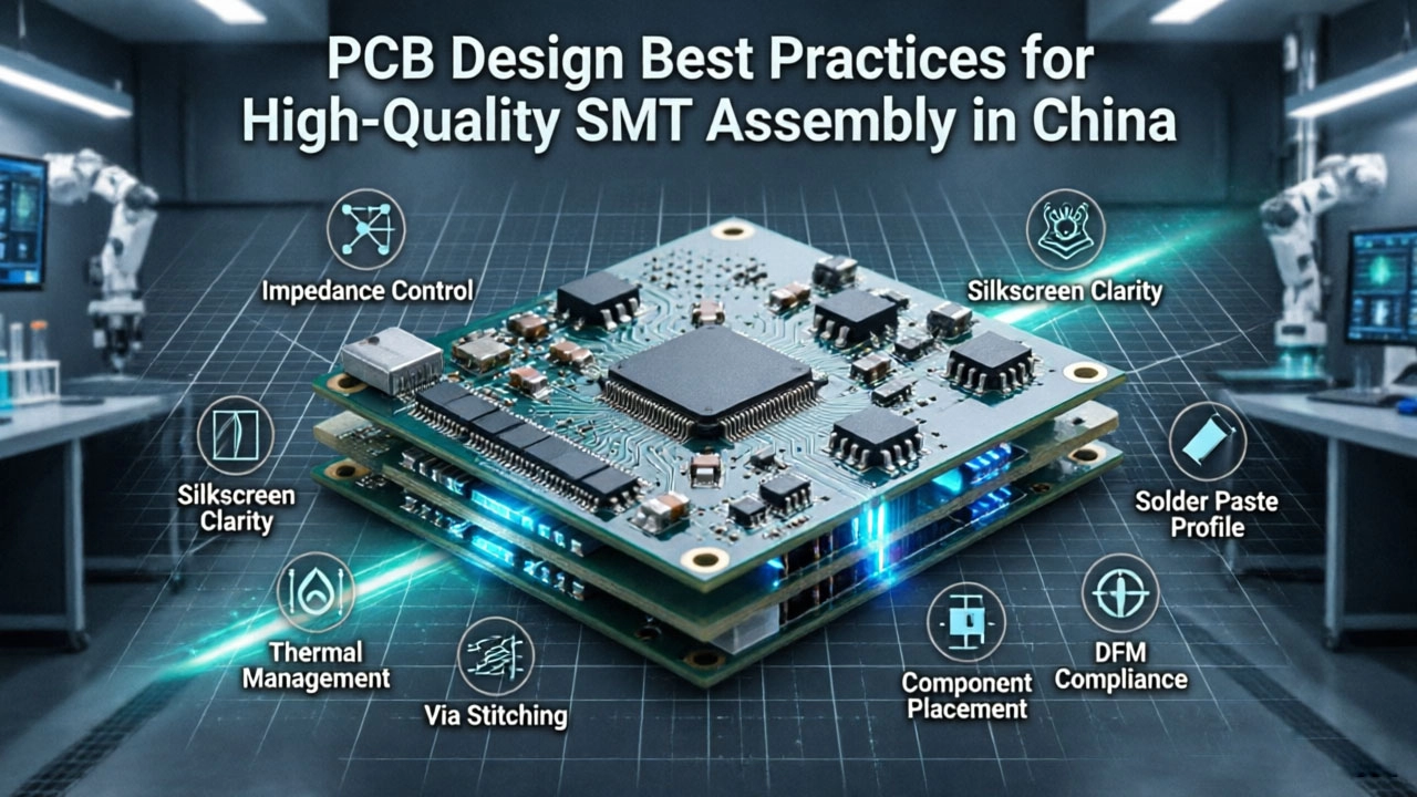
PCB Design Best Practices for High-Quality SMT Assembly in ChinaJune/05/2026China remains a global powerhouse for electronics manufacturing, boasting highly automated Surface Mount Technology (SMT) lines capable of producing millions of units with incredible precision. However, the high-speed, fully automated nature of these SMT lines means that even minor design flaws ca...
PCB Design Best Practices for High-Quality SMT Assembly in ChinaMay/29/2026China has become the world's electronics manufacturing powerhouse, but getting high-quality SMT assembly from Chinese facilities requires more than just sending design files. The difference between designs that assemble smoothly and designs that create problems comes down to following best practic...
Key design considerations include selecting appropriate materials, such as FR-4 with a suitable Tg value (e.g., ≥135°C for lead-free processes), and defining standard board thicknesses like 1.6mm to ensure structural stability. Designers must utilize standardized component footprints (e.g., 0603, 0805) and optimize pad geometries to prevent soldering defects during reflow. Additionally, incorporating clear silkscreen markings for component orientation and maintaining adequate spacing between parts are crucial for automated assembly and post-production testing. By integrating these Dfm principles, engineers can significantly enhance production yields, reduce turnaround times, and ensure the overall reliability of the final PCBA products.