Open Nav

Sending your design to a Chinese Smt Assembly house should be straightforward. You export files from your EDA tool, attach them to an email, and wait for boards. Except it rarely works that smoothly. Missing files, inconsistent data, ambiguous component specifications, and formatting that the manufacturer can't parse—these problems delay quotes, corrupt production data, and sometimes result in boards that don't match your intent.
The gap between what you think you sent and what the manufacturer received is where most handoff problems live. Chinese assembly houses have specific expectations about file formats, naming conventions, and data organization that differ from what Western engineers typically assume. Bridging this gap isn't hard, but it requires knowing what's expected and checking that you've provided it.
This guide walks through the practical steps of preparing Gerber files and bill of materials for a China Smt Assembly partner, with Dfm considerations that prevent common problems.
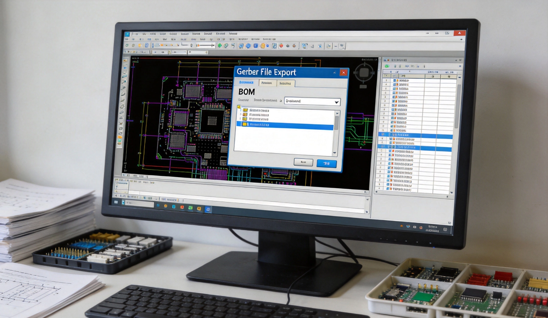
Gerber files define the physical structure of your PCB—copper layers, solder mask, silkscreen, drill data, and board outline. Your assembly house needs these to fabricate the bare boards before populating them with components. Getting them right is the first step to a successful build.
At minimum, your fabrication package must include every copper layer in your design, solder mask for both top and bottom, silkscreen (or legend) for component identification, the board outline defining the board shape, and drill files specifying all holes. Missing any of these creates ambiguity that delays your order or forces the manufacturer to make assumptions.
Common omissions include the board outline (designers assume the manufacturer will derive it from copper, which they can but shouldn't have to), internal layer solder mask (needed if internal layers have exposed pads for press-fit connectors), and blind/buried via drill files (separate files for each drill span, not just one combined drill file).
Chinese manufacturers typically process your files through CAM software that identifies layers by filename patterns. Using standard naming conventions helps their automated systems classify files correctly. While naming standards vary, a common convention uses abbreviations like GTL for top copper, GBL for bottom copper, GTS for top solder mask, GBS for bottom solder mask, GTO for top silkscreen, and GBO for bottom silkscreen.
Avoid generic names like "layer1.ger" that don't indicate which layer the file represents. Even if your EDA tool's default naming seems clear to you, confirm that your manufacturer can interpret it. When in doubt, ask what naming convention they prefer—they'll appreciate the question more than receiving files they need to manually sort.
Gerber format parameters—unit system (metric or imperial), coordinate format (number of integer and decimal digits), and zero suppression (leading or trailing)—must be consistent across all files in the package and must be specified clearly. Most modern Gerber generators use the X2 format with embedded format statements, which eliminates ambiguity. If you're using the older RS-274D format without format statements, you must communicate the format explicitly.
Common problems arise when one file uses 3.3 format (3 integer digits, 3 decimal places) and another uses 3.4, or when some files use metric and others use imperial. These inconsistencies cause the CAM software to mis-scale features, producing boards that don't match your design. Verify format consistency before sending files.
Drill files require special attention. Provide separate drill files for each drill span if your design uses blind or buried vias. A single drill file with all via sizes doesn't convey which vias penetrate which layers—information essential for HDI fabrication.
Include drill start and stop layer information for non-through-hole vias. Most EDA tools can export this information, but it's not always included by default. Check your export settings. The manufacturer needs to know that a 6-mil drill from layer 1 to layer 3 is different from a 6-mil drill from layer 1 through all layers.
Also verify that your drill file includes tool definitions—mapping drill tool numbers to diameters. Without tool definitions, the manufacturer doesn't know what size each drilled hole should be. This information is typically in a separate tool list file or embedded in the drill file header.
The bill of materials tells the assembly house what to put on the board. A poorly prepared BOM is the single most common cause of assembly errors—and most of these errors are preventable with careful preparation.
Every BOM line item must include the reference designator (matching your design schematic and Pcb Layout), the component description or part name, the manufacturer part number (MPN), the quantity per board, and the component package or footprint designation. Missing any of these creates ambiguity that requires manual clarification, delaying your order.
The MPN is particularly critical. It's the unambiguous identifier that allows procurement to source exactly the right part. Vague descriptions like "10K resistor" or "100uF capacitor" are insufficient—there are hundreds of 10K resistors and 100uF capacitors with different packages, tolerances, voltage ratings, and temperature coefficients. The MPN specifies exactly which one you intend.
Component availability is volatile. The part you designed around may be out of stock when your boards are ready for assembly. Providing approved alternatives in your BOM gives the manufacturer flexibility to substitute without waiting for your approval, which saves days on your timeline.
Format alternatives as additional columns or a separate section in the BOM. Clearly indicate which parameters must match for a substitution to be acceptable. For example, a resistor alternative must have the same resistance, tolerance, and package; a capacitor alternative must have equal or higher voltage rating and the same capacitance and package.
Be realistic about what constitutes a valid alternative. A policy of "any 10K 0402 resistor" gives the manufacturer maximum flexibility but risks performance variation if different resistor technologies have different high-frequency behavior or temperature coefficients. Specify the level of equivalence you require.
Chinese assembly houses generally accept BOMs in Excel (.xlsx or .xls) or CSV format. Excel is preferred because it preserves formatting and is easier for their procurement team to review. CSV works but requires consistent delimiter usage (comma-separated, not semicolon or tab).
Structure your BOM with one component per row. A row with multiple reference designators (R1, R2, R3, R4, R5) and one MPN is acceptable and actually preferred—it groups identical components efficiently. Avoid one row per reference designator when many components are identical; this creates unnecessary BOM length that makes review harder.
Include a header row with clear column labels. "Ref Des," "MPN," "Description," "Qty," and "Package" are standard and unambiguous. Avoid abbreviations that might not be recognized internationally.
Beyond Gerber and BOM, the assembly process requires data that tells the pick-and-place machine where each component goes:
The centroid file (also called pick-and-place file or XY data) specifies the X-Y position, rotation, and layer (top or bottom) for every component on the board. This data drives the automated assembly equipment. Without it, the manufacturer must generate placement data manually from your Gerber files—a process that introduces errors and delays.
Verify that your centroid file uses a coordinate origin consistent with your Gerber files. If your Gerber origin is at the lower-left board corner but your centroid file uses a different origin (center of board, for example), components will be placed at wrong positions. Most EDA tools use the same origin for both, but it's worth verifying, especially if you've changed origin settings during design.
Rotation values in centroid files must follow the convention your manufacturer expects. Rotation conventions vary between EDA tools—some define zero rotation differently for different component types, and some use counter-clockwise rotation while others use clockwise. Ask your assembly partner what convention they prefer, and verify that your export matches.
An assembly drawing provides a visual reference that helps the manufacturer verify Component Placement, polarity, and orientation. It's not strictly necessary if your centroid file and BOM are perfect, but it serves as a valuable check that catches errors in the machine data.
The assembly drawing should show component outlines with reference designators, polarity indicators for polarized parts (diodes, electrolytic capacitors, ICs with pin 1 marking), and any special assembly instructions (thermal pad solder requirements, specific solder paste amounts, or components that require hand placement after automated assembly).
Before packaging your files and sending them to your manufacturer, perform your own Dfm review. Catching problems at this stage is free; catching them after the manufacturer's CAM review costs time; catching them after production costs money.
Solder paste openings that don't match component pads. Your solder paste Gerber should define paste openings consistent with your component land patterns. Missing or incorrect solder paste data forces the manufacturer to generate stencil data from the copper pads, which may not match your intent for components requiring reduced or enlarged paste deposits.
Components placed too close to board edges for automated assembly. Pick-and-place machines and reflow ovens require some board edge clearance. Components within 3 to 5 millimeters of the board edge may interfere with conveyor rails or panel tooling. This is especially relevant for small boards that are panelized—components near the individual board edge may be fine if the panel edge has adequate clearance.
Fiducial Marks missing or insufficient. Fiducials—reference marks used by the pick-and-place machine for board alignment—are essential for automated assembly. Provide at least three fiducials on the top side and three on the bottom if you have bottom-side components. Global fiducials (on the panel) and local fiducials (near fine-pitch components) serve different purposes and both may be needed.
Test points inaccessible or undefined. If your design includes in-circuit test points, verify they're accessible from the test side and documented in a separate test point list. Random via pads aren't reliable test points—the manufacturer needs to know which points are intended for testing and their expected net connections.
How you package and deliver your files affects processing speed:
Organize files in a clear folder structure. One folder for Gerber fabrication data, one for assembly data (centroid, BOM), one for any special instructions or reference documents. Don't mix everything into a single flat directory.
Include a readme file documenting what each file contains, any special requirements, and contact information for technical questions. This is simple but remarkably effective at preventing confusion.
Use standard file formats. Gerber RS-274X (with embedded aperture definitions) is preferred over the older RS-274D format. ODB++ or IPC-2581 are acceptable if your manufacturer supports them, and they provide more integrated data than separate Gerber files. Check what formats your manufacturer accepts before choosing.
Compress your file package into a single ZIP archive for transfer. Don't send files individually as email attachments—parts get separated, renamed, or lost. A single ZIP file preserves your folder structure and ensures everything arrives together.
Cultural and language differences add complexity to technical communication. Practical steps that help:
Use simple, direct English in technical correspondence. Avoid idioms, slang, and ambiguous phrasing. "The board needs Fiducial Marks on both sides" is clear. "We want fiducials all around" is ambiguous.
Confirm receipt of your files and ask for confirmation that they can be processed. Don't assume silence means everything is okay. Request a CAM review report that identifies any issues before production begins. Most manufacturers provide this service, and the review often catches problems that would otherwise cause delays.
Be available to answer questions promptly. Time zone differences of 8 to 12 hours mean that a question sent during their workday arrives during your night. If you can't respond until your next morning, that's a full day lost. Establish a communication cadence—perhaps a brief daily check of email or messaging platform—so questions get answered within hours rather than days.
RS-274X (extended Gerber) with embedded aperture definitions is the most widely supported format and is recommended for most designs. ODB++ or IPC-2581 provide more integrated data but confirm that your manufacturer supports them before using these formats.
If you have specific primary and secondary sources, list the preferred MPN as primary and alternatives in a separate column. If you're flexible on source, provide the most common MPN and note that equivalents are acceptable with your approval.
Yes, especially if your design has components requiring non-standard paste amounts—QFN thermal pads, through-hole paste-in-hole, or components needing reduced paste to prevent tombstoning. If you don't provide solder paste data, the manufacturer will generate it from copper pad data, which may not match your requirements.
Rename the files to match the manufacturer's expected convention before sending. Most EDA tools allow you to configure output file naming, or you can rename files after export. The few minutes spent renaming prevents confusion on the receiving end.
It's not required for assembly, but 3D STEP files of the board can help the manufacturer verify component clearance and fit, particularly for tall components or designs with mechanical constraints. If you have them, include them—they cost nothing to share and may prevent assembly issues.
Contact us to discuss your requirements.
Essential DFM Guidelines for SMT PCB Assembly in ChinaJune/04/2026

Understanding IPC Standards in DFM for SMT PCB Assembly China ProjectsSeptember/08/2026

Communicating DFM Rules Effectively with Your SMT PCB Assembly China PartnerAugust/03/2026

Optimizing PCB Design for Chinese SMT ManufacturersJuly/02/2026

How DFM Analysis in China Can Prevent Costly SMT Assembly DelaysAugust/14/2026

Optimizing Component Spacing and Land Patterns for Flawless SMT Assembly in ChinaSeptember/18/2026
Top 10 DFM Mistakes to Avoid Before Sending Files to China for SMT AssemblyJuly/14/2026

The Role of SMT Assembly in China's Modern Industrial Automation and Robotics SectorAugust/08/2026