Open Nav

If you have never worked with a Contract Manufacturer in China before, the first article inspection process can feel opaque. You submitted your design files, your Bom, and your assembly drawings. The boards came back and look fine on the surface. But what exactly did the manufacturer check, and how do you know whether the inspection they performed is rigorous enough to catch the problems that would surface later — in functional test, in the customer's hands, or in the field? This article walks through the first article inspection process in detail, explaining what happens at each stage, what the acceptance criteria are, and what you should look for when reviewing the FAI report from a Chinese assembly partner.
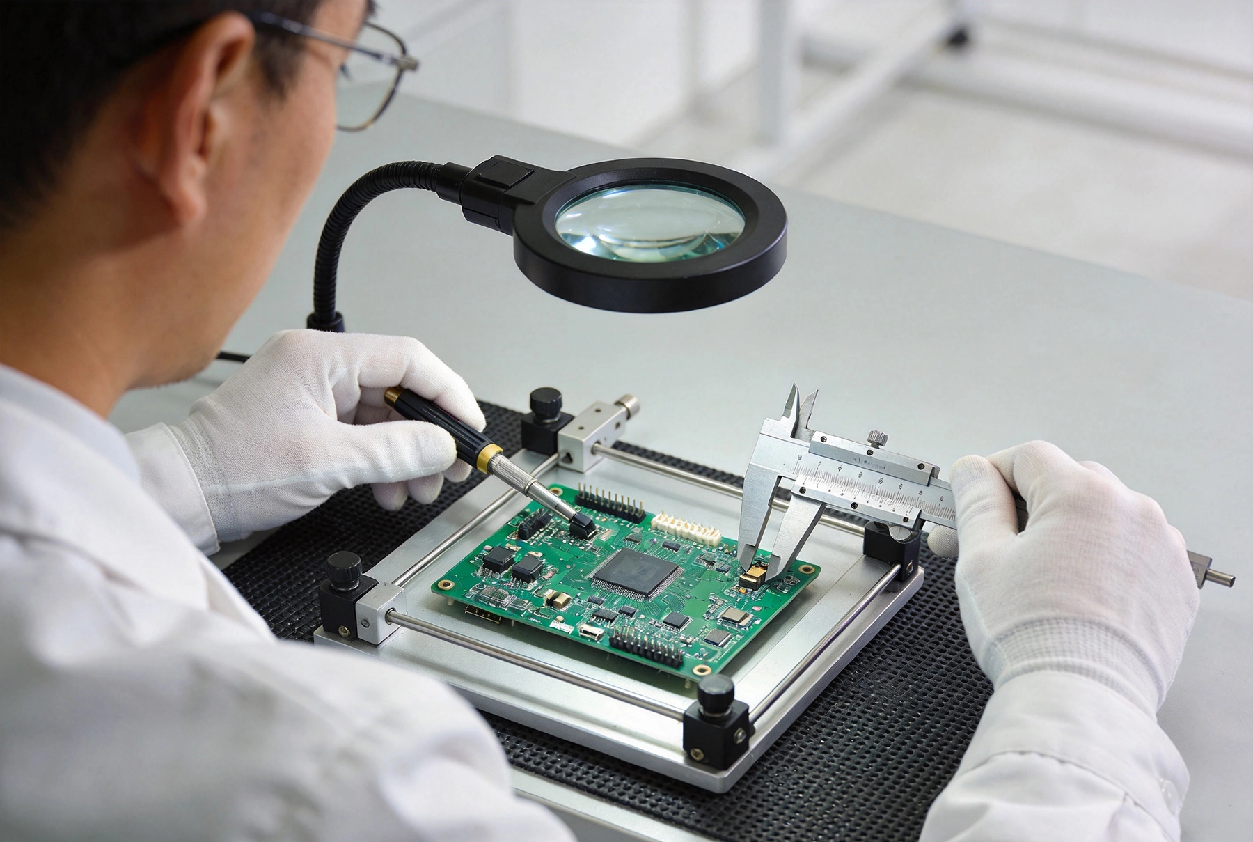
First article inspection is a comprehensive examination of the first units produced in a new production run or after a significant design change. The term comes from the aerospace and defense industries, where it is defined in standards such as AS9100, but the concept applies broadly across all Electronics Manufacturing. The purpose of the FAI is to verify that the manufactured product conforms to the design intent — that the parts placed are the correct parts, that the solder joints meet the quality standards, that the board dimensions are within tolerance, and that the board performs its intended electrical function.
For SMT PCB Assembly in a China factory context, the FAI is typically performed on 1 to 5 boards from the first production lot before the remainder of the order is released to completion. If the FAI reveals issues, those issues are documented, root cause analysis is performed, and corrective actions are taken before the rest of the boards are assembled. This prevents a situation where an entire production run of hundreds of boards has a systematic defect that was present from the start but went undetected.
In a typical Turnkey Assembly engagement with a Chinese manufacturer, the FAI is performed by the manufacturer's quality team using their inspection equipment and procedures. The customer — you — then receives an FAI report documenting the results. Some customers choose to have a third-party inspection service perform an independent FAI, either at the factory or at a local receiving inspection facility. For high-reliability applications in medical, automotive, or aerospace, independent third-party inspection is common practice and is often required by the customer's quality system.
The key point is that the manufacturer's internal FAI is not the same as an independent qualification. A thorough FAI process includes the customer's right to review and approve the inspection criteria, access to the raw inspection data, and a defined escalation path for resolving disagreements about whether a finding constitutes a defect.
Before any physical inspection begins, the FAI team verifies that the boards were built from the correct documentation. This includes checking that the Bom used matches the approved BOM, that the component lot numbers and date codes are acceptable, that the fabrication data matches the approved stackup specification, and that any special processing requirements — such as moisture-sensitive component handling, Conformal Coating, or special cleaning — were followed.
BOM verification is one of the most commonly skipped steps in informal FAI processes, but it is also one of the most important. A single wrong component on the BOM — a resistor with the wrong value, or an IC from the wrong manufacturer — can cause the board to fail in ways that are expensive to diagnose and repair. A thorough FAI will cross-check every component on the board against the BOM, either by visual inspection of markings, by electrical measurement of passive components, or by scanning the component barcodes and verifying them against the approved BOM.
The first physical inspection step is a visual examination of the assembled board, typically using an optical microscope or an Automated Optical Inspection (Aoi) system. The inspector checks for:
For boards with fine-pitch components — BGAs, 0.4 mm pitch QFNs, 0201 passives — visual inspection alone is insufficient, and the FAI must include additional inspection methods that can see beneath the component body.
Area array packages like BGAs and some QFN packages have solder joints that are completely hidden beneath the component body. No amount of optical magnification will reveal whether the solder joint under a BGA is properly formed, has voids, has bridging between adjacent balls, or has sufficient collapse to form a reliable connection. X-ray Inspection is the standard tool for evaluating hidden solder joints, and it is an essential element of any FAI for boards that include BGAs.
X-ray Inspection of BGA joints evaluates several key parameters:
Scanning acoustic microscopy (SAM) is used on some FAI programs to check for delamination or voids in the board substrate — particularly important for HDI boards or boards that have undergone rework. However, SAM is more commonly used for specific failure investigation than for routine FAI, and its inclusion in a standard FAI scope should be negotiated with the manufacturer if your design has specific delamination risk.
Visual and X-ray inspection verify that the board looks correct. Electrical testing verifies that the board functions correctly. The electrical test scope for an FAI typically includes several levels:
Continuity and isolation testing: Each net in the design is tested to verify that it is electrically continuous (not open) and that adjacent nets are properly isolated (not shorted). This test is performed using a flying probe tester or an in-circuit tester (ICT). Flying probe is the more common choice for prototype and low-volume FAI because it does not require a custom test fixture; ICT is more common for high-volume production because it tests multiple boards simultaneously.
Power-on functional test: For boards that have a defined functional behavior — a power supply that outputs a regulated voltage, a motor controller that responds to input signals, a sensor module that produces a calibrated output — the FAI should include a power-on functional test that verifies this behavior. A board that passes continuity testing but fails functional test has a design or assembly issue that must be resolved.
Boundary scan testing: For boards with JTAG-capable ICs (common in complex digital designs), boundary scan testing can verify the interconnections between JTAG devices without requiring a full in-circuit test fixture. This is particularly valuable for boards with BGA packages that cannot be probed directly.
Some FAI programs include dimensional verification of the assembled board — measuring overall board dimensions, hole diameters, slot dimensions, and the positions of critical features such as mounting holes, connectors, and Fiducial Marks. This is more common for boards with tight mechanical fit requirements — for example, a board that must drop into a specific enclosure with minimal clearance.
Dimensional verification is also important for boards that will be wave soldered or press-fit assembled, where the hole sizes and positions must be within tight tolerances to ensure correct insertion and solder fillet formation.
If the FAI includes any special processes — Conformal Coating, potting, programming of flash or FPGA devices, flash calibration, end-of-line labeling — the FAI should verify that these processes were performed correctly on the first article boards. Conformal coating coverage and thickness, potting void content, programmed device contents, and labeling accuracy are all items that should be checked and documented.
Once the FAI is complete, the manufacturer issues a report documenting the findings. A good FAI report is detailed, objective, and actionable. Here is what to look for when you receive the report.
The report should classify each finding by type and severity. IPC-A-610 defines defect classifications that are widely used in the industry:
Be cautious of a manufacturer that reports only a pass/fail result without providing the detailed defect classification and the specific IPC criteria used to evaluate each finding. A vague "FAI passed" result with no supporting data is not a meaningful FAI report.
A quality FAI report includes photographic evidence of all significant findings — images of any defect locations, X-ray images of any BGA anomalies, and images of any special process results. Photographs allow you to independently evaluate whether the classification is correct and to compare the findings against your own acceptance criteria. A report without photographs is difficult to evaluate and provides limited value for customers who are not present at the factory during the inspection.
For any major defect identified in the FAI, the manufacturer should provide a root cause analysis — an explanation of why the defect occurred — and a corrective action plan that describes what will change in the process to prevent recurrence. A corrective action that addresses only the symptom (for example, reworking the defective boards) without addressing the root cause (for example, improving stencil alignment) will not prevent the same defect from occurring on subsequent boards.
The FAI boards themselves become part of the qualification record. The question of whether the FAI boards should be included in the production shipment or held as reference samples should be agreed upon before the FAI begins. For high-reliability applications, keeping the FAI boards as reference samples allows future lots to be compared against the approved first article — a practice that is standard in aerospace and Automotive Quality systems.
If the Aoi or X-ray inspection reveals that components are consistently offset from their target positions — but not enough to cause a solder joint failure — the root cause is typically a problem with the pick-and-place machine's calibration or an issue with the centroid file used to program the placement. The corrective action is machine recalibration or centroid file correction. A consistent offset that is within the IPC-A-610 tolerance for minor defects may be accepted for the current lot, but the root cause must still be corrected for subsequent production.
If the X-ray inspection reveals BGA voiding above the agreed-upon threshold, the root cause is typically an issue with the solder paste formulation, the stencil aperture design, or the Reflow Profile. Voiding can often be reduced by adjusting the soak zone in the Reflow Profile, reducing the ramp rate through liquidus, or changing the solder paste to a formulation with a lower tendency to outgas. The FAI should be repeated after the corrective action to verify that the voiding has been brought within acceptable limits.
Open joints on fine-pitch components — especially QFN packages with center thermal pads — are typically caused by insufficient solder paste volume, poor pad wetting, or a reflow profile that does not achieve adequate solder wetting. The corrective action may involve stencil redesign, pad surface preparation, or profile adjustment. Any open joint detected in the FAI is a major defect that requires corrective action before production continues.
If the BOM verification reveals a component discrepancy — a part that was ordered but not the part specified in the approved BOM — this is a critical finding that requires immediate escalation. The affected boards must be quarantined, the BOM must be corrected, and the root cause of the discrepancy must be identified and corrected. If the wrong component has already been assembled into boards, those boards must be reworked or scrapped.
The FAI process is most effective when it is defined in advance, before the first production order is placed. Here are the key elements to negotiate with your Chinese assembly partner before you submit your first order.
Agree on the IPC-A-610 class that applies to your boards before the order begins. If your product is a consumer device, Class 2 is typically appropriate. If it is a medical or automotive component with higher reliability requirements, specify Class 3 and define any additional customer-specific requirements that go beyond the IPC standard.
Specify what inspection methods are included in the FAI, what sample size will be inspected (typically 100 percent for small lots, statistical sampling for larger lots), and what the acceptance criteria are for each method. If you have BGA packages, specify that X-ray inspection of all BGA joints is required. If you have specific functional test requirements, specify the test procedure and the acceptance criteria.
Request the specific data fields that you want in the FAI report — defect counts by type, photographic evidence of all major findings, measured void percentages for BGA joints, TDR impedance test results if applicable. A manufacturer that has difficulty providing a structured report format may not have the documentation discipline that high-reliability applications require.
Establish in advance what happens when a major defect is found. Who makes the decision to hold the production run? What is the timeline for root cause analysis and corrective action? Who approves the re-inspection? Having these agreements in place before the problem occurs prevents confusion and delays when a critical FAI finding comes in.
The first article inspection is the most important quality gate in an Smt Assembly run. It is the moment when potential problems are identified before they can propagate into an entire production lot. A rigorous, well-documented FAI process — with clear acceptance criteria, photographic evidence, root cause analysis for any defects, and a defined escalation process — gives both the customer and the manufacturer confidence that the production run is proceeding correctly.
Working with a Chinese assembly partner that treats FAI as a genuine quality control tool rather than a compliance checkbox requires upfront investment in defining the scope, the criteria, and the escalation process. That investment pays for itself the first time an FAI catches a systematic defect before hundreds of boards are assembled with the same problem.
Contact us to discuss your requirements.

Wave Soldering vs. Reflow: Navigating the SMT PCB Assembly Process in ChinaAugust/12/2026

How China's SMT PCB Assembly Process Meets International IPC-A-610 StandardsJuly/22/2026
How to Place Fiducial Marks for Accurate SMT PCB Assembly in ChinaAugust/15/2026

The Complete Process WalkthroughMay/29/2026

How a Top High Frequency PCB Manufacturer Ensures Signal IntegrityJune/02/2026
Understanding Reflow Soldering Profiles Used in SMT PCB Assembly ChinaJune/30/2026

The Importance of X-Ray Inspection for BGA in China's SMT Assembly ProcessAugust/03/2026

The Role of Automated Optical Inspection (AOI) in China's SMT Assembly LinesJune/16/2026