Open Nav
In the world of advanced electronics, signal integrity has become one of the most critical factors determining system performance. From 5G communication networks to automotive radar systems, from satellite communications to medical imaging equipment, high frequency applications demand PCB designs that can transmit signals with minimal distortion, loss, and interference. This is why choosing the right high frequency PCB manufacturer matters more than ever before.
Signal integrity refers to the ability of a signal to maintain its original waveform and timing characteristics as it travels through a printed circuit board. When signals operate at frequencies above 1 GHz, traditional Pcb Manufacturing approaches often fall short. The physical characteristics of the board—trace geometry, dielectric properties, impedance control, and material selection—become as important as the circuit design itself.
In this comprehensive guide, we explore the key strategies and processes that leading high frequency PCB manufacturers employ to ensure exceptional signal integrity in every board they produce.
Before diving into solutions, it's essential to understand why signal integrity becomes so challenging at high frequencies. When signal frequencies increase, several physical phenomena come into play that can severely degrade performance if not properly managed.
At high frequencies, signals experience greater attenuation as they travel along traces. This loss occurs due to both conductor losses (skin effect) and dielectric losses. The skin effect causes current to concentrate on the surface of conductors, increasing effective resistance. Dielectric loss, on the other hand, converts signal energy into heat within the substrate material. Top manufacturers address these issues through careful material selection and trace design optimization.
When the impedance of a trace varies along its path—due to inconsistent trace width, improper grounding, or inadequate planning—signal reflections occur. These reflections can cause data errors, reduce signal amplitude, and create standing waves that distort the original signal. Professional high frequency PCB manufacturers use controlled impedance design to maintain consistent impedance throughout the signal path, typically targeting 50 ohms for RF applications.
High speed signals can couple energy into neighboring traces, causing unintended interference. This crosstalk becomes particularly problematic in dense PCB designs with many parallel traces running at high frequencies. Manufacturers employ various techniques including proper trace spacing, ground plane segmentation, and differential pair routing to minimize this effect.
High frequency signals naturally radiate electromagnetic energy, which can interfere with other components both on and off the board. Without proper shielding and grounding strategies, EMI can compromise system reliability and regulatory compliance. Leading manufacturers implement comprehensive EMI reduction measures throughout the manufacturing process.
The dielectric material used in a high frequency PCB fundamentally determines its electrical performance. Unlike standard FR-4 materials designed for lower frequency applications, high frequency boards require substrates with specific electrical properties.
Top manufacturers work with advanced materials such as Rogers RT/duroid, Taconic RF substrates, and ceramic-filled PTFE composites. These materials offer several advantages for high frequency applications:
A professional high frequency PCB manufacturer evaluates materials based on the specific application requirements. For 5G infrastructure, materials like Rogers RO4003C offer excellent high frequency performance with the processing advantages of traditional thermoset laminates. For aerospace and defense applications requiring extreme performance, ultra-low loss materials such as Rogers RO3003 or ceramic-filled PTFE substrates provide the best signal transmission characteristics, even though they present more challenging manufacturing requirements.
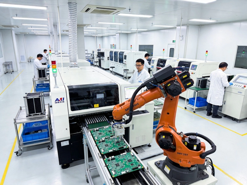
Material selection provides the foundation, but manufacturing precision determines whether that potential is realized in the finished product. Leading manufacturers invest heavily in advanced equipment and process controls to achieve the tolerances required for high frequency applications.
Maintaining consistent trace impedance requires precise control over multiple manufacturing parameters. This includes:
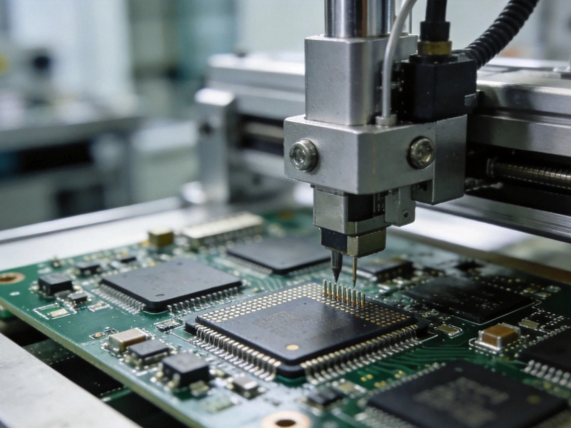
Vias represent one of the most critical—and challenging—aspects of high frequency Pcb Design. Inductive and capacitive effects in vias can severely degrade signal quality. Professional manufacturers employ several strategies to minimize via impacts:
The surface condition of copper traces directly affects high frequency performance. Manufacturers use sophisticated cleaning and surface treatment processes to ensure optimal conductor characteristics. Controlled atmosphere storage and processing prevent oxidation that could affect impedance consistency.
The most successful high frequency PCB projects involve close collaboration between designers and manufacturers from the earliest stages. Top manufacturers offer comprehensive Dfm services that help optimize designs for both performance and producibility.
Before committing to production, experienced engineers review designs for potential signal integrity issues. This review typically addresses:
Creating the optimal layer stack-up is crucial for high frequency performance. Manufacturers work with customers to determine the ideal combination of dielectric materials, prepreg types, and layer thicknesses that achieve target impedance values while meeting mechanical and thermal requirements.
Established manufacturers maintain libraries of validated trace geometries and configurations for common impedance values (50 ohm single-ended, 90 ohm differential, 100 ohm differential). These proven designs can significantly accelerate development timelines while ensuring first-pass success.
Even the most precise manufacturing process requires verification. Leading high frequency PCB manufacturers employ sophisticated testing methodologies to ensure every board meets stringent signal integrity requirements.
TDR testing provides detailed characterization of impedance variations along traces. This non-destructive testing method sends a fast rise-time pulse through a trace and analyzes reflections to identify discontinuities, impedance mismatches, and manufacturing variations. Professional manufacturers perform TDR testing on sample boards from every production lot to verify process consistency.
Vector network analyzers (VNAs) measure S-parameters (scattering parameters) to characterize how signals behave at various frequencies. Key measurements include:
High magnification optical and electron microscopy reveals manufacturing defects that could affect signal integrity. Inspectors examine trace geometry, plated via quality, delamination, and other potential issues that might not be visible to the naked eye.
Beyond high frequency characterization, comprehensive electrical testing verifies:
Technical capabilities alone don't guarantee excellent signal integrity. The accumulated knowledge and experience of an organization's engineering team plays an equally important role. Here's why choosing an experienced manufacturer matters:
Signal integrity at high frequencies involves complex electromagnetic interactions. Experienced engineers understand how design choices affect wave propagation, radiation, and coupling phenomena. They can anticipate potential issues and recommend solutions based on similar projects they've successfully completed.
Years of manufacturing high frequency PCBs provide invaluable feedback for process improvement. Manufacturers who have produced thousands of RF and microwave boards have refined their processes to consistently achieve tight tolerances and exceptional quality. This institutional knowledge translates into better outcomes for customers.
Established manufacturers maintain strong relationships with premium material suppliers, ensuring access to the highest quality substrates. These relationships also provide advantages in material allocation during supply chain constraints—critical for time-sensitive projects.
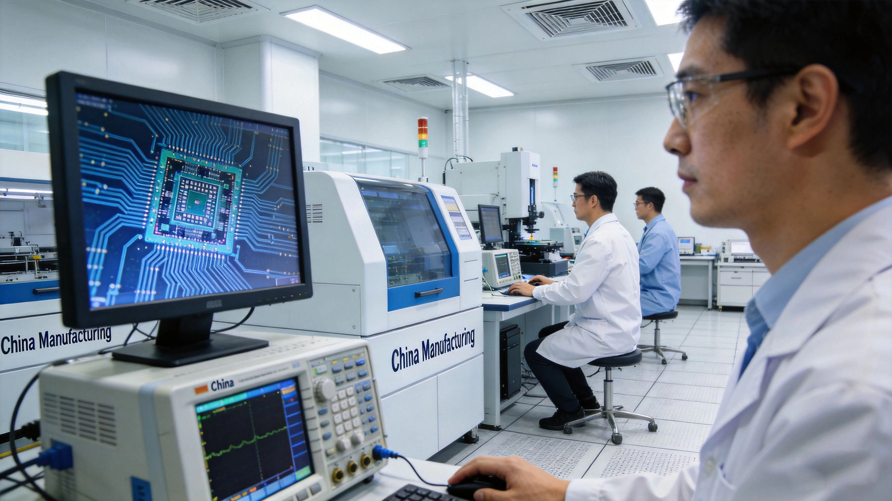
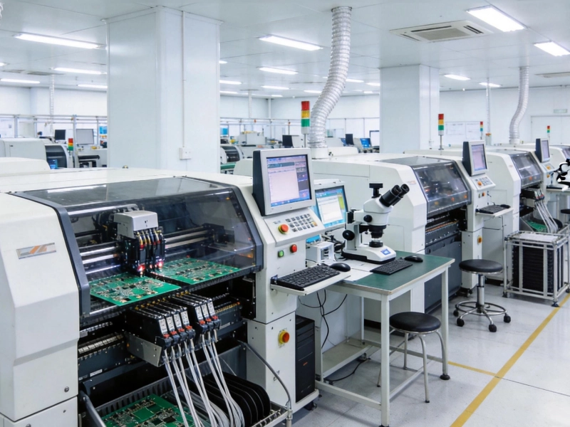
Over the past two decades, China has established itself as a global leader in advanced Pcb Manufacturing, including high frequency applications. Several factors contribute to this leadership position:
With many options available, how do you select the right partner for your high frequency PCB needs? Consider these factors:
Evaluate the manufacturer's technical specifications against your requirements. Key questions include:
Look for relevant certifications including ISO 9001, AS9100 (aerospace), Iatf 16949 (automotive), and ITAR registration for defense applications. These certifications indicate systematic quality management and consistent processes.
Excellent technical support and clear communication are essential for complex high frequency projects. Evaluate response times, technical expertise of sales and support staff, and willingness to collaborate on design optimization.
Ensure the manufacturer can meet your volume requirements and delivery schedules. Understand their production capabilities, current lead times, and ability to scale if needed.
Ensuring signal integrity in high frequency PCBs requires a comprehensive approach combining advanced materials, precision manufacturing, rigorous testing, and deep expertise. From material selection through final inspection, every step in the process must be optimized for high frequency performance.
Working with an experienced, capable high frequency PCB manufacturer can make the difference between a project that meets specifications on the first try and one that requires multiple iterations and costly delays. By understanding the factors that contribute to signal integrity and selecting a manufacturing partner who excels in each of these areas, you can confidently bring your high frequency designs from concept to production.
Whether you're developing 5G infrastructure, automotive radar systems, satellite communications equipment, or any other application requiring exceptional high frequency performance, the right manufacturing partner will help ensure your products deliver the reliability and performance your customers expect.
Leading manufacturers typically achieve impedance tolerances of ±5% or better for high frequency applications. Some specialized processes can achieve ±2% tolerance, though this requires additional validation and may affect production lead times and costs.
Material selection depends on your specific application requirements including operating frequency, temperature range, power handling, mechanical constraints, and budget. Rogers and Taconic materials offer excellent performance but at higher costs than standard materials. An experienced manufacturer can recommend the optimal material for your requirements.
At minimum, request TDR testing for impedance verification and continuity testing for all nets. For critical applications, consider requesting full S-parameter characterization using a vector network analyzer, microscopic inspection, and thermal cycling testing.
High frequency PCBs typically cost 2-5 times more than equivalent standard boards due to specialized materials, tighter tolerances, and additional testing requirements. However, the performance benefits often justify this investment for applications where signal integrity is critical.
Lead times vary based on complexity, material availability, and manufacturer capacity. Standard high frequency boards might require 2-3 weeks, while complex designs with specialized materials or tight tolerances could require 4-8 weeks or more.
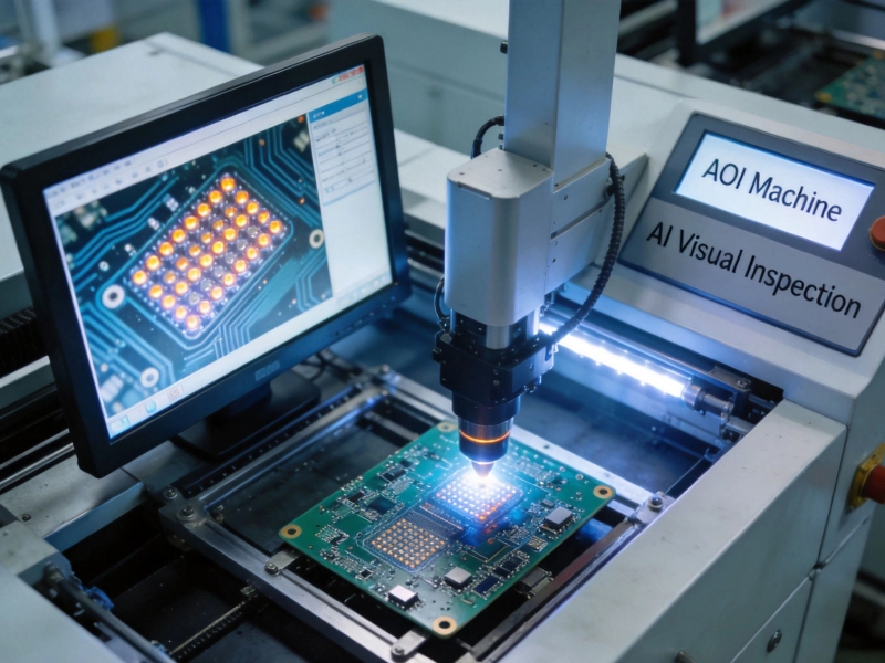
The Role of Automated Optical Inspection (AOI) in China's SMT Assembly LinesJune/16/2026
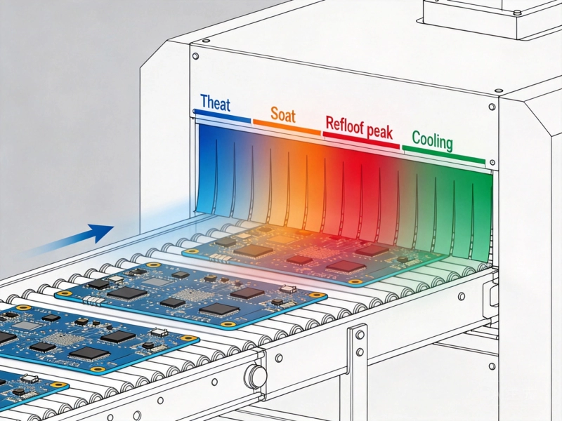
Understanding Reflow Soldering Profiles Used in SMT PCB Assembly ChinaJune/30/2026
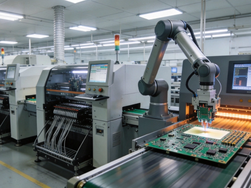
Step-by-Step: From Solder Paste Printing to Final Testing in China SMT AssemblyJuly/13/2026
The Complete Process WalkthroughMay/29/2026
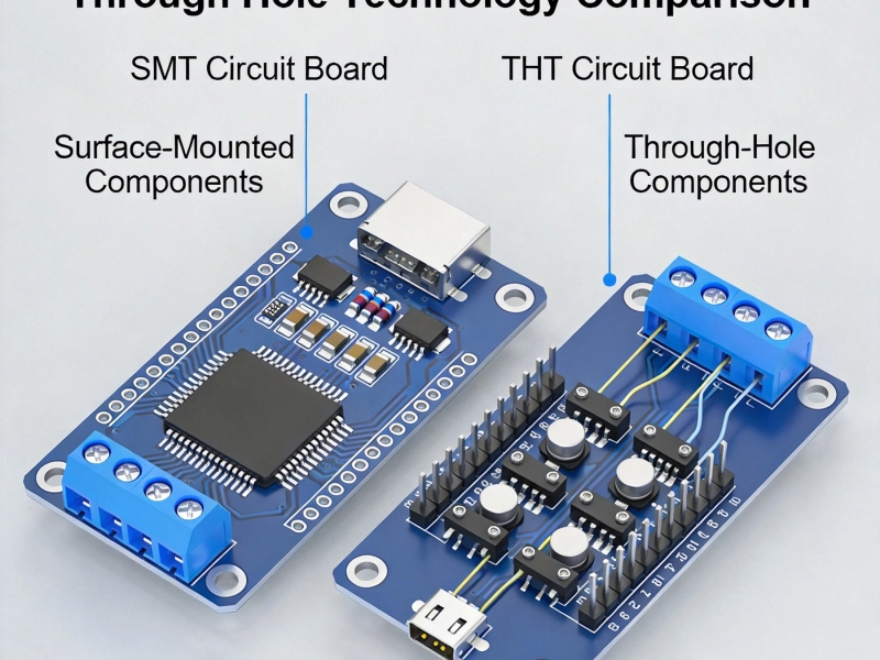
Which Technology is Right for Your Project?May/29/2026
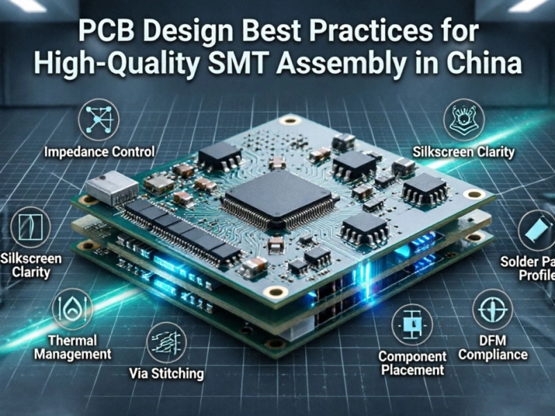
PCB Design Best Practices for High-Quality SMT Assembly in ChinaJune/05/2026
Customizing SMT PCB Assembly China Applications for High-Density Interconnect (HDI) BoardsJune/22/2026
Industrial SMT PCB Assembly in China: Meeting Durability and Reliability StandardsJune/11/2026