Open Nav

Tombstoning is one of the most annoying defects in Smt Assembly. A small resistor or capacitor stands up on one end like a tiny tombstone, breaking the circuit and forcing rework. The problem is especially common with 0402, 0201, and other small passive components, but it can happen on larger packages too if the layout or process is not balanced.
If you are sourcing PCBA from China, avoiding tombstoning requires more than just good design rules. You also need clear communication with your assembly partner, realistic pad designs, controlled Solder Paste Printing, and a Reflow Profile that matches the actual board. This article shares practical Pcb Design tips to reduce tombstoning risk in passive Smt Assembly, especially for teams working with Chinese PCBA suppliers.
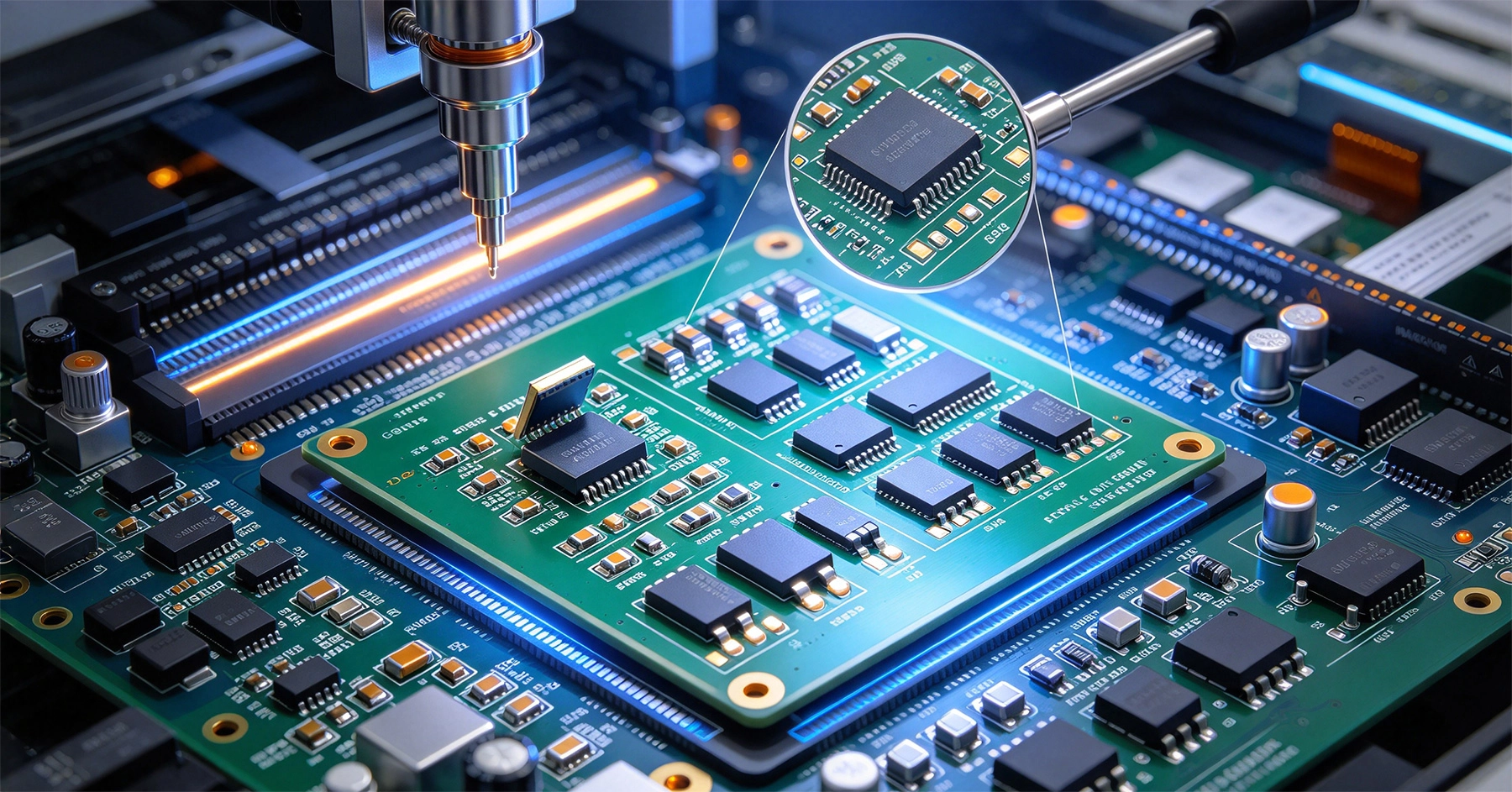
Tombstoning, also called the Manhattan effect, occurs when one end of a surface-mount passive component lifts off the pad during reflow. It happens mainly because of uneven surface tension. When solder paste on one pad melts earlier or wets faster than the other side, the molten solder pulls the component upward.
The root causes usually include:
In many cases, tombstoning is not caused by a single mistake. It is a combination of layout, paste printing, placement, and reflow. That is why prevention should start at the Pcb Design stage.
Pad design is the first line of defense against tombstoning. If the two pads are not symmetrical, the component will almost always have a higher risk of standing up during reflow.
Both pads should have the same length, width, and shape. Even a small difference can create uneven wetting force. For 0402 and 0201 resistors and capacitors, symmetry matters more than you might think.
Larger pads hold more solder paste, which increases surface tension during reflow. If one pad is connected to a large copper area and the other is not, the imbalance becomes worse. Do not make pads bigger just to "make assembly easier."
Use pad dimensions recommended by the component supplier, the assembly house, or Ipc-7351 as a starting point. For high-volume production, it is better to confirm pad sizes with your China PCBA partner because their stencil thickness, printer capability, and reflow equipment may affect the optimal layout.
Thermal imbalance is one of the most common causes of tombstoning. If one pad connects directly to a large ground plane or thermal relief is missing, that side may heat more slowly. The other pad may reach reflow temperature earlier, causing the component to rotate or lift.
Practical thermal balance tips:
In one 0402 decoupling capacitor layout, moving a thermal via away from the left pad and adding a matching thermal relief on the right pad reduced tombstoning from several percent to nearly zero. The schematic was fine, but the copper layout created a clear thermal imbalance.
Even a perfect pad layout can fail if the solder paste volume is uneven. Stencil design plays a huge role in preventing tombstoning, especially for small passives.
The stencil apertures for both pads should be identical. Do not enlarge one side to "ensure enough solder." That often makes the problem worse.
For 0201 and 0402 components, a slightly reduced aperture can help. Many assembly houses use home-plate or rounded-rectangle apertures instead of full-size square openings. This reduces excess solder and lowers the pulling force during reflow.
Common stencil thicknesses are 0.10 mm, 0.12 mm, and 0.15 mm. Thicker stencils deposit more paste, which may increase tombstoning risk for very small components. Your China Assembly supplier can recommend the best thickness based on your component mix.
Expired solder paste, poor storage, or inconsistent printing can all increase defects. If you are working with a PCBA factory in Shenzhen, Dongguan, or other manufacturing hubs, ask about their solder paste management process. It sounds basic, but it matters alot.
Placement accuracy affects tombstoning more than many designers realize. If a component is slightly rotated or shifted before reflow, one end may wet earlier than the other. For 0201 and 01005 Components, even a small offset can cause problems.
Good practices include:
For boards with many small passives, it is helpful to add Fiducial Marks and ensure good panelization. These details help the assembly line maintain registration and reduce placement variation.
Reflow profiling is usually handled by the assembly factory, but designers should still understand the basics. A well-controlled Reflow Profile gives solder paste time to activate flux, collapse evenly, and wet both pads before full reflow.
Key points to discuss with your China PCBA supplier:
If your board has heavy copper areas, large ground planes, or mixed component sizes, ask the factory to run a thermal profile test before mass production. This step can save you from repeating the same tombstoning issue across multiple batches.
Many tombstoning issues can be caught during Dfm review. Before you send Gerber Files, Bom, and pick-and-place data to a PCBA supplier in China, run a few quick checks.
Recommended Dfm checklist:
It is also useful to share your expected production volume, testing requirements, and rework expectations early. A good PCBA partner in China will not just quote price; they should also flag high-risk footprints before production starts.
One pad is larger because the footprint was copied from another design. This creates uneven solder volume and wetting force.
The ground-connected pad absorbs more heat, so the other side melts first and pulls the component up.
More paste does not mean better joints. Excess paste increases surface tension imbalance during reflow.
Using full-size square apertures for 0201 Components often creates too much solder. Aperture reduction or shaping can help.
Assuming the factory will "just fix it" is risky. Tombstoning prevention works best when design, stencil, placement, and reflow are aligned from the beginning.
Small passive components such as 0201, 0402, and some 0603 resistors and capacitors are most at risk. The lighter the component, the easier it is for surface tension to lift one end.
Sometimes, but not always. A better reflow profile can reduce the defect rate, but if the pad design or thermal balance is poor, tombstoning may still occur. Layout changes are often more effective.
In most cases, yes. Symmetrical pads help balance wetting force. If one side must connect to a large copper area, use thermal relief and keep the pad dimensions the same.
Share complete design data, confirm pad sizes and stencil apertures, request Dfm Feedback, and ask for reflow profile validation during Npi. Clear communication is as important as good layout.
Avoiding tombstoning is not about one magic rule. It is about keeping the two ends of a passive component as balanced as possible. Symmetrical pads, balanced thermal paths, controlled solder paste, accurate placement, and a stable reflow profile all work together.
For teams assembling in China, the advantage is that many PCBA suppliers have strong experience with high-mix and high-volume SMT production. The key is to involve them early. Send your Gerber Files, Bom, and assembly notes before mass production, and ask for specific feedback on small passive components. A short DFM discussion can prevent a lot of rework later.
How to Design the Perfect Land Pattern for SMT Components in Chinese FactoriesJune/18/2026
PCB Stack-up Considerations for Reliable SMT PCB Assembly in Chinese Supply ChainsSeptember/20/2026
PCB Panelization Guide for SMT Assembly China: V-Scoring vs. Tab RoutingJuly/03/2026
The Impact of PCB Surface Finish on SMT Assembly Soldering Quality in ChinaAugust/06/2026
Thermal Management in PCB Design: Preventing Warpage in China's SMT AssemblyJuly/15/2026

PCB Design Best Practices for High-Quality SMT Assembly in ChinaJune/05/2026
PCB Design Best Practices for High-Quality SMT Assembly in ChinaMay/29/2026
Designing Mixed-Technology Boards: Integrating THT and SMT Assembly for China ProductionSeptember/09/2026