
The relentless drive toward smaller, lighter, and more feature-rich electronic products has pushed component packaging to its physical limits. Where once 0805 resistors dominated circuit boards, the industry now routinely specifies 0201 (0.6mm × 0.3mm) and 01005 (0.4mm × 0.2mm) components for applications ranging from smartphones and wearables to medical devices and Automotive Electronics. These ultra-miniature parts present significant manufacturing challenges that require careful design consideration, especially when outsourcing assembly to China-based Smt Services. Understanding how to design successfully with these components separates smooth production runs from frustrating yield problems and quality escapes.
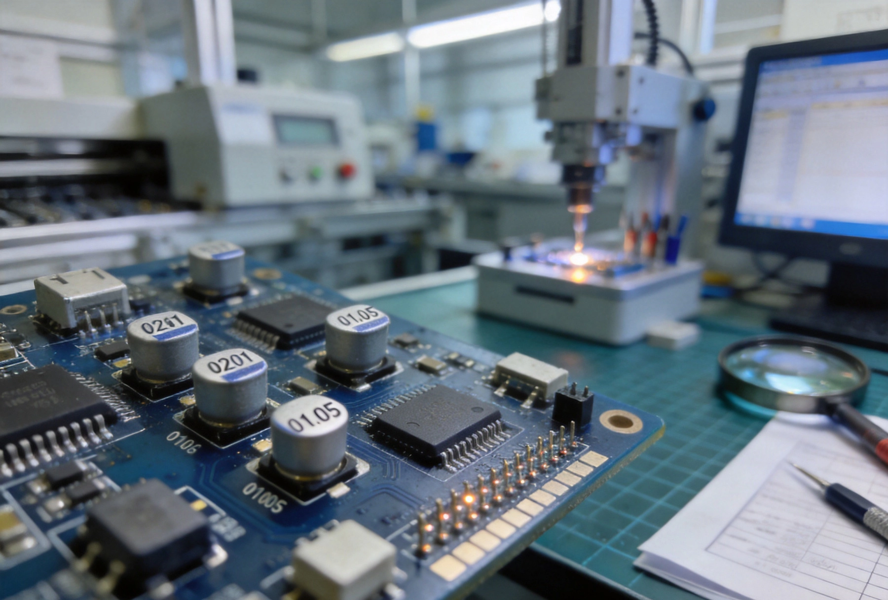
The metric designation for chip components describes dimensions in tenths of millimeters. A 0201 component measures 0.6mm × 0.3mm, while a 01005 shrinks further to just 0.4mm × 0.2mm. To appreciate the scale, a human hair averages about 75 microns in diameter—the 01005 component is less than three times that width. This microscopic scale introduces physics and manufacturing challenges that engineers accustomed to larger packages must understand before specifying these parts.
The industry continues pushing toward even smaller packages like 008004 (0.25mm × 0.125mm), though these remain niche applications outside high-volume consumer products. At current production scale, 0201 and 01005 represent the practical limits for most China-based assembly operations, though not all facilities can reliably handle 01005 components. Selecting the right manufacturing partner requires honest assessment of their equipment capabilities and process experience with fine-pitch components.
Component miniaturization delivers tangible benefits beyond marketing appeal. Smaller packages reduce board area proportionally, enabling smaller end products or more functionality in the same footprint. Reduced lead inductance and resistance improve electrical performance for high-frequency circuits. Lower material content reduces component cost for high-volume applications, though assembly complexity may offset raw component savings. These trade-offs require careful evaluation for each application.
Modern pick-and-place equipment must achieve placement accuracy measured in microns to reliably handle 0201 and 01005 components. Standard placement machines specifying ±0.1mm accuracy struggle with 01005 parts, where pads may be only 0.2mm wide. High-precision pick-and-place systems using vision recognition, laser centering, and advanced nozzle technology can achieve ±0.03mm or better accuracy, enabling reliable placement of the smallest components.
Nozzle selection becomes critical for fine-pitch components. Standard pickup nozzles create excessive vacuum force that can crush or misposition 01005 parts, while worn nozzles cause inconsistent pickup leading to placement errors. Specialized ultra-fine nozzles with controlled vacuum, often using ceramic or carbon fiber materials, provide the precision needed for miniature components. Maintaining nozzle inventory and replacement schedules directly impacts assembly quality.
Solder Paste Printing faces matching challenges at these scales. Stencil apertures for 01005 pads may be less than 0.15mm wide, demanding laser-cut stainless stencils rather than chemically etched alternatives. Squeegee speed, pressure, and separation parameters must be optimized to achieve complete paste release without smearing or bridging. These fine-tuning requirements make stencil specification and printing process setup more involved than for larger components.
Pad design for 0201 components should follow Ipc-7351 generic specifications with adjustments for the specific assembly process. Land pattern dimensions typically target 0.35mm × 0.4mm per pad, providing adequate paste coverage while maintaining appropriate spacing. Solder mask defined pads offer better paste volume control but may stress smaller pads during thermal cycling, while non-solder-mask defined pads provide stronger mechanical attachment at the cost of less precise paste deposition.
Component spacing requirements increase for smaller parts. Minimum clearance of 0.15mm between 0201 bodies prevents pick-and-place interference and provides clearance for Solder Paste Printing between adjacent pads. Some designers specify even larger clearances of 0.25mm or more to improve manufacturing margin and facilitate Automated Optical Inspection. The cost of this spacing in board area must be weighed against improved yield and quality.
Component orientation consistency across the board improves assembly efficiency and inspection accuracy. Placing all resistors and capacitors in the same orientation allows Aoi systems to quickly identify misplaced parts. Documentation should clearly specify orientation requirements, as 0201 components have no polarity but can be placed in four orientations relative to the board, creating potential for confusion in large component counts.
01005 components demand even tighter design rules than 0201 parts. Pad dimensions typically target 0.22mm × 0.2mm per land, leaving minimal margin for placement and paste variation. The ratio between pad width and component body approaches 1:1, meaning any placement error significantly impacts solder joint geometry. Designers should specify maximum tolerances and verify manufacturer capabilities before finalizing pad dimensions.
Clearance between adjacent 01005 components must increase proportionally to prevent placement and solder interaction issues. Minimum clearance of 0.12mm between component bodies provides space for paste printing while preventing pick-and-place nozzle interference. This spacing represents a significant fraction of 01005 body size, limiting how densely these parts can be packed. High-density digital circuits often use 01005 for passive components while using larger packages for active components where footprint allows easier manufacturing.
Thermal relief design for 01005 thermal pads requires careful consideration. Components with thermal pads need via patterns sized appropriately for the smaller geometry, typically 0.1mm diameter or smaller. Microvia-in-thermal-pad configurations may be necessary, adding manufacturing complexity and cost. For prototypes or low-volume production, avoiding thermal pad requirements in 01005 packages simplifies assembly considerably.
Solder alloy selection affects 01005 assembly success significantly. Standard SAC305 (96.5% tin, 3% silver, 0.5% copper) works adequately but may cause issues with tombstoning—the tendency of small components to stand up on one end during reflow. Low-silver alloys like SAC105 or SAC0805 reduce tombstoning risk at the cost of slightly higher melting point. Some manufacturers prefer no-clean formulations that eliminate post-reflow cleaning, though washable pastes may be specified for applications requiring thorough residue removal.
Paste classification for fine-pitch components should use Type 4 or Type 5 powder (25-45 microns or 20-38 microns respectively) rather than coarser Type 3 powder common for larger components. Finer powder enables better paste release from small apertures but requires fresher paste and tighter storage controls. Shelf life limits become more critical, and paste handling procedures must prevent contamination or oxidation that becomes significant at these scales.
Paste volume control for 01005 requires careful optimization. Too little paste creates insufficient solder joints prone to failure, while too much paste causes bridging between adjacent components. The aspect ratio of stencil apertures—width divided by thickness—directly impacts release characteristics, with aspect ratios between 1:1 and 1.5:1 typically providing optimal results. Laser-cut stencils with polished apertures achieve better release than etched stencils for these fine features.
Thermal profiling for fine-pitch assembly requires tighter control than for larger components. The smaller thermal mass of 0201 and 01005 parts means faster temperature ramp rates and shorter soak times can work, but precise control prevents thermal shock that causes component cracking or pad lifting. Modern reflow ovens with multi-zone temperature control and nitrogen atmosphere provide the precision needed for consistent results.
Ramp rates between 1.5°C and 3°C per second typically work well for boards with mixed component sizes. Faster ramp rates risk thermal gradients within components, while slower rates extend time above liquidus when oxidation and intermetallic growth occur. The profile must balance thermal uniformity across the board against total process time that affects throughput.
Peak temperature and time above liquidus (TAL) requirements become more critical with smaller components. Standard profiles targeting 245°C peak with 60-90 seconds TAL work for most SAC alloys, but specific component packages may have tighter limits. Some 01005 components from certain manufacturers specify maximum peak temperatures or TAL values that conflict with standard profiles. Verifying component thermal specifications before assembly prevents surprises.
Automated Optical Inspection (Aoi) becomes both more important and more challenging for assemblies with fine-pitch components. The small feature sizes exceed the resolution capability of standard AOI systems designed for 0402 and larger components. High-resolution camera systems with 10-15 micron resolution are required for reliable 01005 inspection, adding cost and processing time compared to standard inspection.
AOI algorithms must be tuned specifically for 01005 components. Standard libraries expecting larger component silhouettes may misidentify or fail to detect 01005 parts entirely. False rejection rates tend to increase when inspection parameters are not properly configured, causing unnecessary rework and delay. Experienced manufacturers have developed optimized inspection parameters through extensive trial and error.
X-ray Inspection may be necessary for assemblies with hidden solder joints, such as bottom-terminated components or complex BGA patterns adjacent to fine-pitch passives. While 0201 and 01005 components themselves rarely require X-ray Inspection, the capability provides confidence that assembly processes are functioning correctly. Some manufacturers include X-ray sampling as standard quality verification for high-reliability applications.
Tombstoning represents the most characteristic defect for 0201 and 01005 components, occurring when thermal gradients during reflow create surface tension imbalance that lifts one end of the component. Prevention focuses on paste printing uniformity, Component Placement accuracy, and profile optimization. Low-silver solder alloys, nitrogen atmosphere during reflow, and adjusted ramp rates all contribute to tombstoning reduction.
Solder bridging between adjacent components occurs when excessive paste or poor paste release creates unintended connections. The microscopic scale of 01005 spacing makes bridging inspection challenging, and bridges may not be immediately apparent during visual inspection. Paste volume optimization, appropriate stencil thickness, and controlled printing parameters prevent bridging before it starts.
Component cracking from thermal or mechanical stress manifests as intermittent or complete electrical opens. The small size of 01005 components makes them more susceptible to stress cracking than larger packages, particularly at the weak points where component body meets terminations. Handling procedures that prevent mechanical stress during assembly and appropriate thermal profiles that avoid thermal shock reduce cracking risk.
China-based Smt Assembly facilities have invested heavily in equipment for fine-pitch components, driven by demand from Consumer Electronics manufacturers producing smartphones, tablets, and wearables at massive scale. This investment means many facilities can handle 0201 and 01005 assembly, though capability varies significantly. Due diligence before selecting a partner should include verification of actual equipment, process capability documentation, and samples from previous similar work.
Communication challenges sometimes arise with China Manufacturing partners, particularly around fine-tuning parameters for non-standard components. Clear documentation of requirements, acceptance criteria, and process controls reduces misunderstandings. Many successful relationships involve iterative qualification builds where initial assemblies identify issues for process adjustment before production commitment.
Logistics and supply chain considerations affect component selection for China assembly. Shipping 01005 components from international suppliers adds lead time and potential quality risk during transit. Local sourcing through China-based distributors may offer faster delivery but with different Quality Assurance. Balancing component availability against manufacturing capability requires planning that begins before design completion.
Assembly cost for fine-pitch components typically exceeds cost for larger packages due to increased equipment precision, lower yields, and more extensive inspection requirements. 01005 assembly may cost 30-50% more per placement than 0402 components, though raw component cost savings may partially offset this. The total cost equation must include defect rates, rework costs, and potential field failure costs that higher assembly complexity introduces.
Stencil cost increases proportionally with precision requirements. Laser-cut stainless stencils with fine-aperture polish cost substantially more than standard etched stencils, and thinner foils (typically 0.08mm rather than 0.1mm for larger components) wear faster, requiring more frequent replacement. These consumable costs accumulate across production runs and affect per-board pricing.
Yield sensitivity means that small defect rates create larger cost impact than for simpler assemblies. A 1% defect rate on a board with 100 components costs less than a 1% defect rate on a board with 500 components because more defects occur per defect opportunity. For high-volume production, even marginal improvements in first-pass yield can translate to substantial cost savings across total volume.
Component selection between 0201 and 01005 involves trade-offs between size reduction and manufacturing complexity. 0201 components offer approximately 40% area reduction compared to 0402 while maintaining reasonable manufacturing margin with most modern equipment. 01005 components provide another 40% reduction beyond 0201 but require more precise equipment and tighter process control. The marginal benefit of 01005 over 0201 must be weighed against increased manufacturing risk.
Application requirements drive appropriate package selection. Consumer wearables and hearing aids where size truly constrains product design justify the manufacturing complexity of 01005. Industrial and automotive applications where manufacturing robustness matters more than absolute size often favor 0201 or even 0402 packages. Medical devices may require 01005 for implants where space is truly constrained but will accept longer development and higher assembly cost.
Component availability differs between package sizes. 0201 components are available from virtually all passive component manufacturers, with multiple sources for each value. 01005 components have narrower availability, with some values available from single sources. This supply concentration risk may argue against 01005 for applications where supply continuity matters more than absolute size reduction.
Dfm review with manufacturing partners before layout completion identifies potential assembly issues before they become expensive redesigns. Sharing preliminary layout files allows manufacturers to verify spacing, pad design, and thermal considerations against their specific capabilities. This collaboration costs little time but can prevent costly revisions after board fabrication.
Standardized footprint libraries based on manufacturer recommendations ensure pad designs match assembly processes. Using generic IPC footprints without manufacturer-specific adjustment may create marginal or poor solder joints. Libraries developed or verified by manufacturing partners provide confidence that pad design will work with their equipment and processes.
Documentation completeness prevents Manufacturing Errors that disproportionately affect fine-pitch assemblies. Centroid files, bill of materials with manufacturer part numbers, assembly drawings with orientation specifications, and special handling instructions all contribute to correct assembly. Ambiguity that might be tolerable for simpler assemblies becomes critical error sources for 01005 boards.
Package-on-package (PoP) and stacked die arrangements continue enabling functionality growth beyond what traditional 2D board layouts can achieve. These approaches combine miniaturization benefits with increased functionality density, though they introduce their own manufacturing challenges around yield and reliability. The trend toward system-in-package solutions may reduce demand for ever-smaller discrete components while increasing complexity of the packages that remain.
Emerging 008004 components represent the next size reduction beyond 01005, though volume production remains limited to the highest-volume consumer applications. Manufacturing equipment continues advancing to handle these smaller packages, and equipment designed for 01005 can often be upgraded for 008004 capability. Design practices established for 01005 will translate directly to these future generations.
Advances in assembly equipment, solder materials, and inspection technology continue improving manufacturing capability for fine-pitch components. What requires specialized equipment today may become routine capability within a few years as equipment depreciates and is replaced with more capable systems. Designing for current manufacturing reality while maintaining awareness of advancing capabilities positions products for both present success and future improvement.
Designing with 0201 and 01005 components enables the miniaturization that modern electronic products demand, but success requires understanding manufacturing realities that differ significantly from larger component packages. Careful pad design, appropriate spacing, optimized paste and stencil selection, and refined reflow profiles all contribute to assemblies that work reliably. Working with capable manufacturing partners who have demonstrated 01005 experience reduces risk substantially compared to assuming any SMT facility can handle these fine-pitch components.
The decision between 0201 and 01005 packages should weigh actual size constraints against manufacturing complexity and supply chain considerations. For many applications, 0201 provides adequate miniaturization with broader manufacturing capability, while 01005 reserved for applications where absolute size reduction justifies the added complexity. This selective approach often achieves better outcomes than defaulting to the smallest available package.
China-based Smt Assembly services offer excellent capability for fine-pitch components when properly qualified, with equipment and experience comparable to any global competitor. Success with these manufacturers comes from clear communication, thorough documentation, and realistic expectations about manufacturing tolerances and process capabilities. Building these relationships on foundations of mutual expertise and honest capability assessment positions projects for smooth production from prototype through high volume.
What is the main difference between 0201 and 01005 components?
0201 components measure 0.6mm × 0.3mm, while 01005 components are smaller at 0.4mm × 0.2mm. The 01005 package represents approximately 44% smaller area than 0201, though it requires more precise manufacturing equipment and tighter process control. Not all SMT facilities can reliably handle 01005 components.
What equipment is needed to assemble 01005 components?
High-precision pick-and-place systems with ±0.03mm or better placement accuracy, vision recognition for component centering, specialized ultra-fine nozzles, laser-cut stencils with polished apertures, and high-resolution Aoi Inspection systems. Standard equipment designed for 0402 and larger components typically cannot handle 01005 reliably.
How can I reduce tombstoning defects with fine-pitch components?
Tombstoning prevention includes using low-silver solder alloys, ensuring paste printing uniformity, verifying placement accuracy, optimizing Reflow Profile with controlled ramp rates, and using nitrogen atmosphere during reflow when available. Each factor contributes to the thermal balance that prevents component lifting.
Are 01005 components more expensive to assemble than 0201?
Yes, 01005 assembly typically costs 30-50% more per placement than 0201 due to equipment precision requirements, lower first-pass yields, and more extensive inspection. Raw component costs may be lower for 01005, but total cost including assembly favors larger packages when size reduction does not provide critical benefit.
Should I use 01005 components for all miniaturized products?
Not necessarily. 01005 should be reserved for applications where absolute size reduction genuinely matters, such as wearables or medical implants. For most applications, 0201 provides adequate miniaturization with broader manufacturing capability and lower risk. Defaulting to the smallest package increases cost and complexity without proportional benefit.
Designing Mixed-Technology Boards: Integrating THT and SMT Assembly for China ProductionSeptember/09/2026
How to Design the Perfect Land Pattern for SMT Components in Chinese FactoriesJune/18/2026
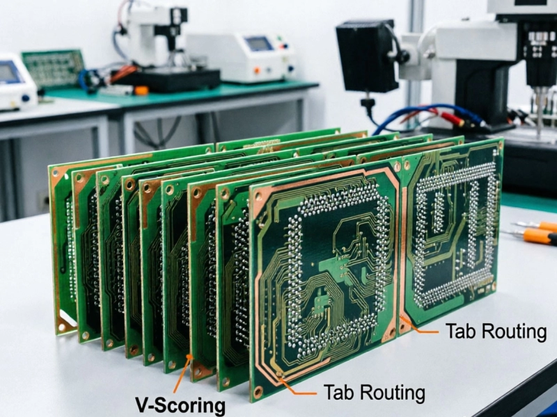
PCB Panelization Guide for SMT Assembly China: V-Scoring vs. Tab RoutingJuly/03/2026
PCB Design Best Practices for High-Quality SMT Assembly in ChinaMay/29/2026
PCB Design Best Practices for High-Quality SMT Assembly in ChinaJune/05/2026
Thermal Management in PCB Design: Preventing Warpage in China's SMT AssemblyJuly/15/2026
The Impact of PCB Surface Finish on SMT Assembly Soldering Quality in ChinaAugust/06/2026
How We Helped a US Startup Scale from Prototype to Mass SMT Assembly in ChinaJuly/07/2026