Open Nav

China has established itself as the world's leading destination for Surface Mount Technology (SMT) assembly, hosting thousands of Electronics Manufacturing services (EMS) providers ranging from small workshops to massive industrial facilities. The country's Smt Assembly capabilities span the full spectrum—from Rapid Prototyping runs to high-volume production lines capable of millions of units monthly. Understanding the step-by-step Smt Assembly process helps product teams navigate manufacturing partnerships more effectively, whether they are sourcing their first prototype or scaling to mass production.
This guide walks through each stage of the SMT assembly process, from initial solder paste application through final functional testing. Each step builds upon the previous one, creating the complete electronic assemblies that power everything from consumer gadgets to industrial equipment.
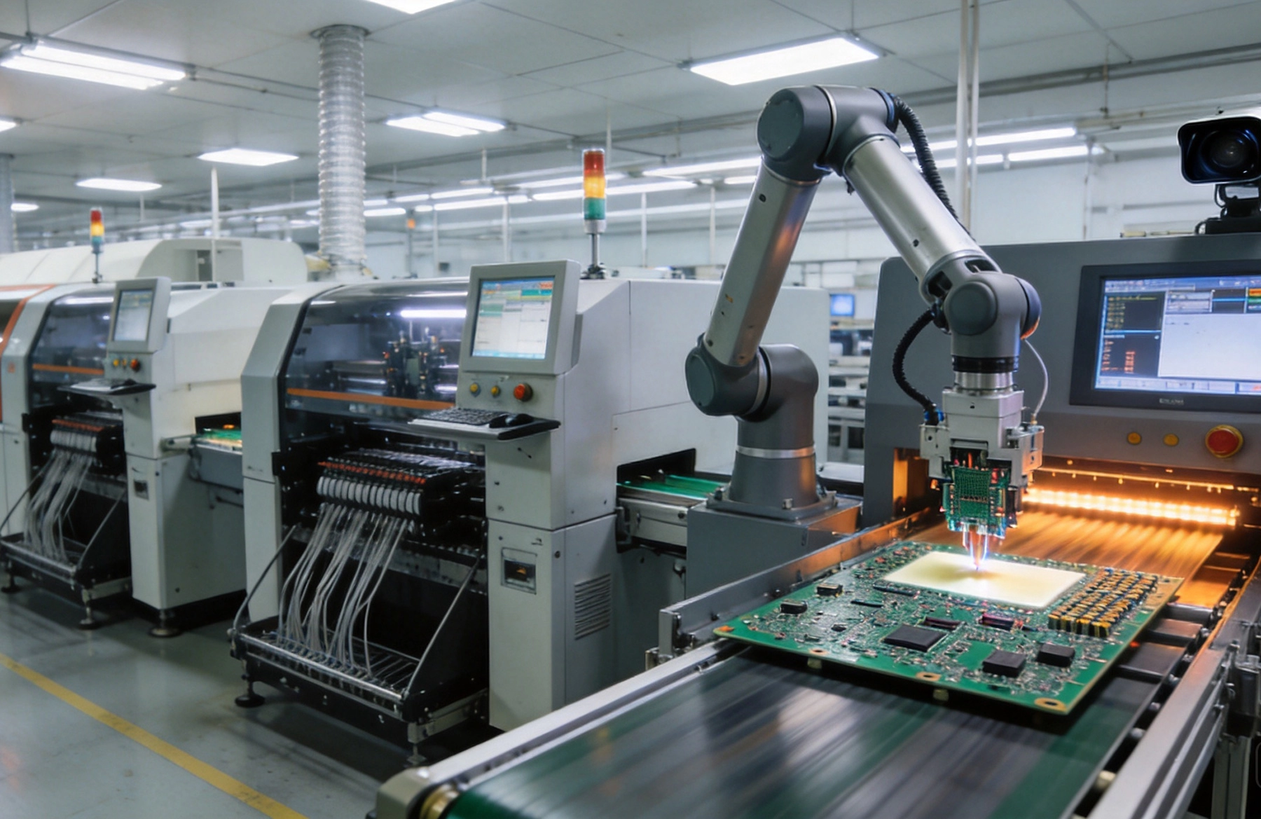
Before any assembly begins, printed circuit boards must be prepared and loaded onto the production line. This preparatory stage establishes the foundation for successful assembly:
Modern SMT lines in China typically use automated handling systems that feed PCBs directly from panel magazines into the production line, minimizing human contact and ensuring consistent processing.
Solder paste application represents one of the most critical stages in SMT assembly. The paste—a mixture of fine solder particles suspended in flux—serves dual purposes: it temporarily holds components in place and creates the metallic bond during soldering. Paste application quality directly determines assembly yield rates.
Solder paste printers use stencils—precision-cut metal sheets with apertures matching component pad patterns—to deposit paste exactly where needed:
Solder paste printing requires precise control of multiple variables:
China's advanced SMT facilities use sophisticated paste printers with closed-loop control, automatically adjusting parameters based on SPI feedback to maintain consistent quality across production runs.
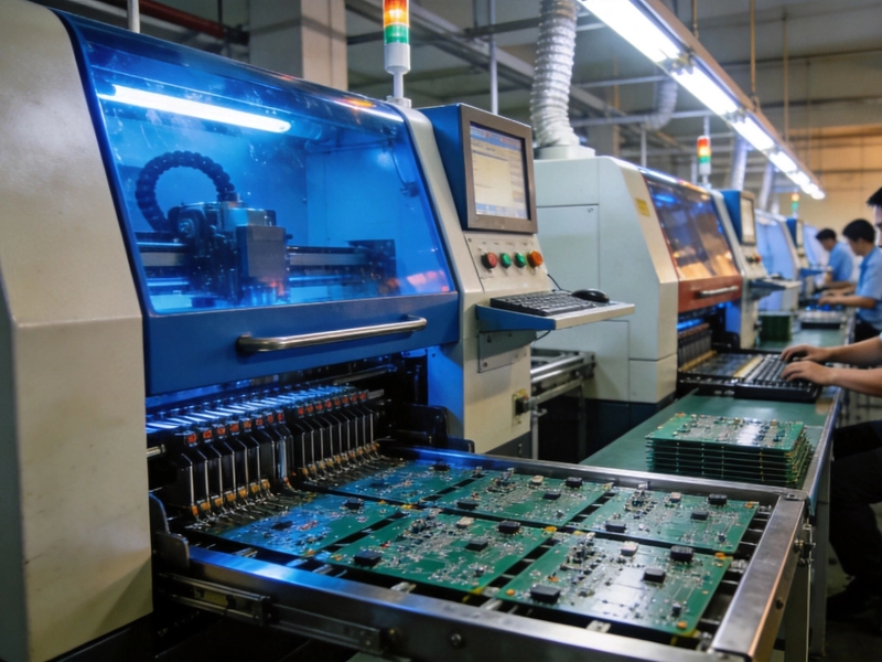
With solder paste deposited on pads, boards move to the pick-and-place stage where Surface Mount components are precisely positioned on the board. This stage transforms bare PCBs into populated assemblies.
Modern placement equipment achieves remarkable speed and accuracy:
Successful Component Placement depends on several interrelated factors:
China's SMT facilities typically operate multiple placement machines in sequence, with high-speed machines handling passives and slower machines placing complex components, optimizing line balance for maximum throughput.
Before full production runs commence, First Article Inspection (FAI) verifies that the setup is correct. This critical checkpoint catches setup errors before they result in defective production runs:
Some facilities use automated in-line inspection systems that provide immediate feedback on placement quality, enabling rapid correction of any detected issues.
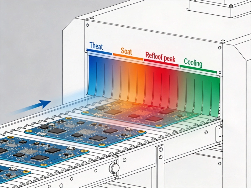
Populated boards then enter the reflow oven, where controlled heating transforms solder paste from a temporary adhesive into permanent metallic connections. Reflow Soldering represents the heart of the SMT assembly process.
Modern reflow ovens contain multiple temperature zones, each serving a specific purpose:
Each board assembly requires a tailored Reflow Profile based on:
China's leading SMT facilities use multi-zone reflow ovens with precise temperature control and nitrogen atmospheres, reducing oxidation and improving solder wetting for high-reliability applications.
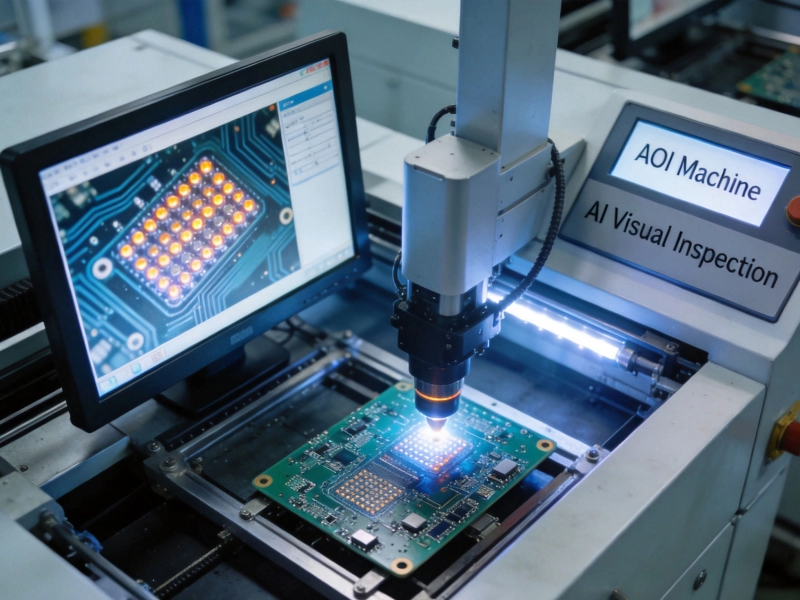
After reflow, boards pass through Automated Optical Inspection systems that detect defects invisible to human inspectors. Aoi represents a critical quality control checkpoint.
Aoi systems examine multiple aspects of solder joints and Component Placement:
Modern AOI systems employ multiple inspection technologies:
While AOI catches the majority of defects, some problems—especially hidden solder joints under BGAs or QFNs—require X-ray Inspection for complete verification.
For assemblies with hidden solder joints—ball grid arrays (BGAs), quad flat no-leads (QFNs), and other bottom-terminated components—X-ray Inspection provides visibility into connections invisible to optical systems:
X-ray inspection adds cost and cycle time, so manufacturers typically use sampling plans rather than 100% inspection. Critical applications like automotive or Medical Electronics often require X-ray verification of all BGA joints.
Many assemblies include both Surface Mount and through-hole components. Through-hole parts require additional assembly processes:
The sequence varies depending on thermal sensitivity—some manufacturers place through-hole components before reflow, while others complete all SMT processing before wave soldering.
Defects identified during inspection require repair. Skilled technicians use specialized rework equipment to correct problems without damaging surrounding components:
Effective rework requires experienced technicians and well-maintained equipment. China has developed substantial expertise in rework operations, with many facilities employing dedicated rework teams for complex defect remediation.
The final stage verifies that assemblies function as designed. Functional testing validates electrical performance before shipment:
Functional tests range from basic continuity checks to comprehensive performance verification:
Effective testing balances coverage against cost and cycle time:
China's manufacturing facilities offer various testing capabilities, from basic ICT and FCT to sophisticated burn-in testing and environmental stress screening for high-reliability applications.
For applications requiring enhanced reliability, assemblies undergo post-assembly processing:
The assembly process concludes with final verification and proper packaging:
China's leading SMT facilities track comprehensive quality metrics:
World-class SMT operations typically achieve FPY above 98%, with target DPMO below 500 for critical applications.
The SMT assembly process represents a carefully orchestrated sequence of stages, each building upon the previous one to create functional electronic assemblies. From precise solder paste application through final testing, every step requires proper execution and quality verification to ensure reliable finished products.
China's SMT assembly industry has developed comprehensive capabilities spanning the entire process chain. Understanding these stages helps product teams communicate more effectively with manufacturing partners, specify appropriate quality requirements, and navigate the complexities of electronics production.
Whether sourcing prototypes for development or establishing mass production for market launch, familiarity with SMT assembly processes enables better decision-making throughout the product lifecycle.
First-pass yield rates at quality-focused China SMT facilities typically exceed 98%, with world-class operations achieving 99%+ for straightforward assemblies. Yield varies based on board complexity, component density, and testing requirements. High-complexity boards with fine-pitch components may see slightly lower yields during initial production until processes stabilize.
Assembly cycle time depends on board complexity and facility capacity. Simple assemblies might complete within 24-48 hours at express facilities. Standard production typically requires 5-10 working days including Component Procurement. Complex assemblies with long-lead components or extensive testing may require 2-3 weeks.
Standard testing usually includes AOI (Automated Optical Inspection) and basic functional testing. ICT (in-circuit test) and FCT (functional circuit test) are common add-ons. X-ray inspection is typically quoted separately and applied based on board complexity or quality requirements. Discuss specific testing needs during quotation to ensure proper process planning.
Quality Assurance strategies include: requesting facility certifications (ISO 9001, Iatf 16949 for automotive), reviewing quality metrics and defect rates, providing clear documentation (Bom, Gerber Files, assembly drawings), requesting First Article Inspection before production, establishing clear acceptance criteria, and maintaining open communication about quality issues.
Common defects include solder bridges (unintended connections between pads), insufficient solder joints, tombstoning (component lifting from one end), component shift during reflow, solder voids under BGAs, and missing components. Quality-focused manufacturers use SPI for paste inspection and AOI for post-reflow verification to catch these defects before shipment.
The Importance of X-Ray Inspection for BGA in China's SMT Assembly ProcessAugust/03/2026
The Complete Process WalkthroughMay/29/2026
What to Expect During the First Article Inspection (FAI) of Your SMT PCB Assembly in ChinaSeptember/30/2026
Wave Soldering vs. Reflow: Navigating the SMT PCB Assembly Process in ChinaAugust/12/2026
Understanding Reflow Soldering Profiles Used in SMT PCB Assembly ChinaJune/30/2026
How to Place Fiducial Marks for Accurate SMT PCB Assembly in ChinaAugust/15/2026
How China's SMT PCB Assembly Process Meets International IPC-A-610 StandardsJuly/22/2026
The Role of Automated Optical Inspection (AOI) in China's SMT Assembly LinesJune/16/2026