Open Nav

Surface Mount Technology has revolutionized Electronics Manufacturing, enabling the Miniaturization and complexity that characterizes modern electronic devices. At the heart of Smt Assembly lie two primary soldering methods: Reflow Soldering and wave soldering. Each process offers distinct advantages and limitations that make it suitable for different applications, component types, and production scenarios. Understanding these differences is essential for engineers and procurement professionals sourcing Pcb Assembly Services in China, where both methods are extensively employed to serve global electronics markets.
China's Electronics Manufacturing industry has invested heavily in both wave soldering and reflow equipment, developing expertise across the full spectrum of SMT capabilities. This infrastructure enables Chinese Contract Manufacturers to serve diverse market segments, from high-volume Consumer Electronics to specialized industrial and medical devices. The choice between wave and Reflow Soldering significantly impacts cost, quality, and production flexibility, making it one of the most consequential decisions in planning Pcb Assembly projects.
This comprehensive guide examines both soldering processes in detail, comparing their mechanisms, capabilities, and optimal applications. By understanding the technical fundamentals and practical trade-offs, you can make informed decisions when engaging with Chinese Smt Assembly partners, ensuring that your projects receive the most appropriate manufacturing approach for their specific requirements.
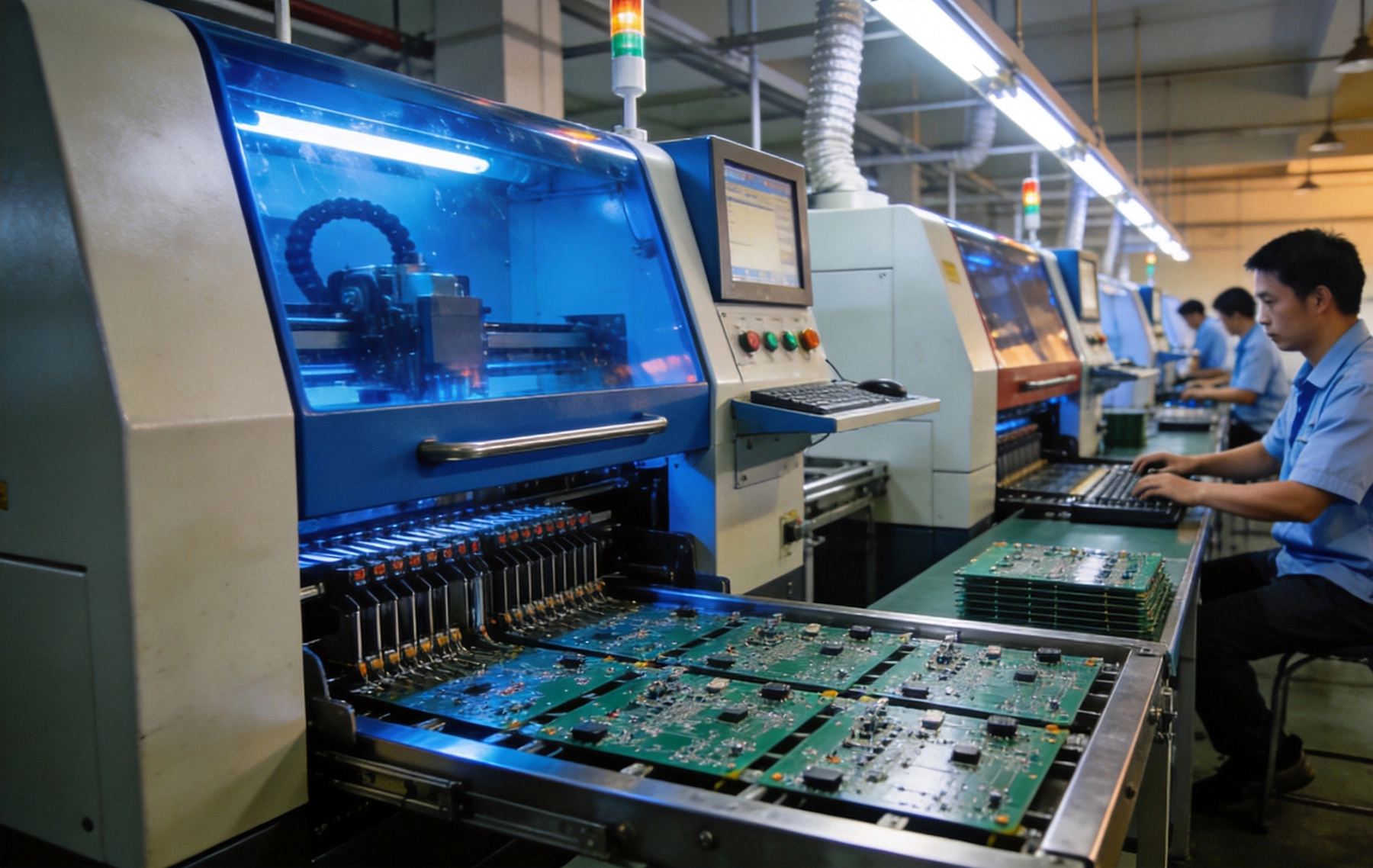
Reflow soldering represents the dominant method for attaching Surface Mount components to PCBs in modern electronics manufacturing. The process involves applying solder paste to PCB pads, placing components on the paste, then heating the entire assembly in a controlled thermal profile that melts the solder and creates permanent connections. This method excels at simultaneously soldering large numbers of components with exceptional consistency, making it ideal for high-volume production of dense, complex assemblies.
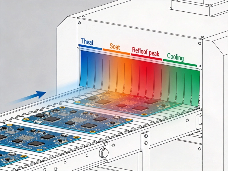
The reflow process achieves its results through carefully engineered thermal profiles that progress through distinct phases. The initial preheat stage gradually raises the board temperature to prevent thermal shock to components and evaporate solvents in the solder paste. The soak phase maintains temperature to achieve uniform heating across the board and activate flux. The peak or reflow phase briefly exceeds the solder melting temperature to form reliable joints, followed by controlled cooling that solidifies the solder without creating thermal stress.
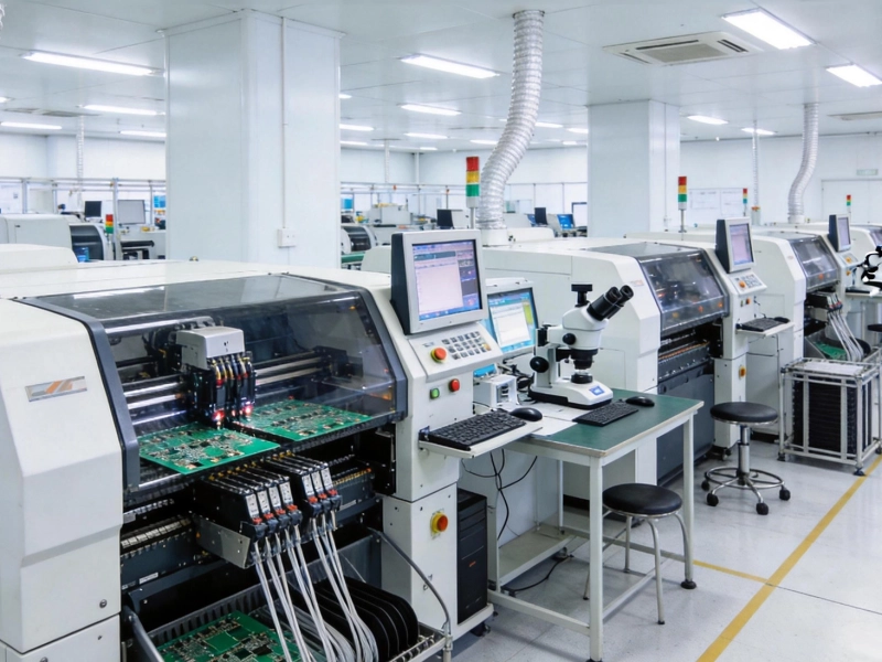
Modern reflow ovens employ forced convection heating that ensures uniform temperature distribution across the entire board surface. Advanced models feature multiple heating zones, precise temperature sensors, and sophisticated control systems that maintain thermal profiles within tight tolerances. Nitrogen atmosphere options reduce oxidation and improve solder wetting for demanding applications. These capabilities enable Chinese SMT lines to achieve the process control necessary for fine-pitch components and lead-free solder alloys.
The primary advantage of reflow soldering lies in its ability to solder all components simultaneously. Once the board passes through the reflow oven, all joints are formed in a single thermal cycle, eliminating the sequential processing that slower methods require. This parallel processing enables exceptionally high throughput, with modern reflow lines handling hundreds of boards per hour depending on thermal profile requirements and board size.
Reflow soldering provides superior control over solder paste deposition when combined with precision stencil printing. Solder paste volume can be accurately controlled through stencil thickness and aperture design, enabling consistent joint formation even for components with varying pad sizes. This consistency supports high first-pass yields that reduce rework costs and improve production efficiency.
The enclosed environment of reflow ovens protects boards from airborne contamination during soldering. Components are fully encapsulated in solder from all accessible angles, creating robust joints with excellent fillet formation. This comprehensive coverage proves particularly valuable for components with multiple leads or pads where complete solder fill is essential for reliability.
Reflow soldering faces challenges with bottom-terminated components that have no exposed leads or terminations beneath their bodies. BGA packages, QFN devices, and other bottom-terminated components create hidden joints that are impossible to inspect visually after reflow. While X-ray Inspection can verify these joints, the hidden nature of potential defects increases Quality Assurance complexity.
Thermal profiling for reflow soldering must accommodate all components on the board, creating challenges when components with vastly different thermal mass share the same assembly. Large connectors or transformers may require customized thermal profiles or special handling to prevent overheating of smaller temperature-sensitive components. This constraint can limit production flexibility and increase setup requirements.
Void formation in solder joints represents a quality concern for reflow assemblies. Trapped gases from solder paste solvents or component outgassing can create voids that weaken joints and reduce thermal and electrical conductivity. While some voiding is acceptable, excessive voids may compromise reliability, particularly for Power Electronics applications where thermal performance is critical.
Wave soldering addresses the specific challenges of through-hole component assembly through a fundamentally different mechanism. Rather than applying heat to the entire board, wave soldering creates a standing wave of molten solder that contacts the underside of the PCB, filling holes and creating solder fillets on component leads. This localized application of solder enables efficient processing of boards with through-hole components while avoiding the thermal exposure that reflow would subject all components to.
The wave soldering process begins with flux application that cleans surfaces and prepares them for solder wetting. The board then passes over a wave of molten solder, typically at temperatures around 260-280 degrees Celsius. Capillary action draws solder up through the holes, creating connections between component leads and PCB pads. The board exits the wave with clean filleted joints on the solder side, ready for inspection and any necessary touch-up.
Modern wave soldering systems incorporate multiple waves—a turbulent chip wave for efficient hole filling and a smoother laminar wave for creating cosmetically superior fillets. Titanium pallet systems prevent solder from adhering to designated areas, while nitrogen atmospheres reduce oxidation and improve wetting. Flux systems have evolved from standalone applicators to integrated systems with precise spray control and automated concentration management.
Wave soldering excels at through-hole component assembly, providing robust mechanical connections that resist vibration and thermal cycling stress. The solder filling holes and creating fillets around leads creates joints significantly stronger than surface-only connections. This mechanical advantage makes wave soldering essential for components that experience physical stress or require exceptional reliability.
The selective nature of wave soldering, processing only the board bottom where holes exist, minimizes thermal exposure to components on the top side. This selective processing enables wave soldering of assemblies that include temperature-sensitive components that could not survive full reflow profiles. Connectors, transformers, and other components with plastic insulators often require this selective processing approach.
Wave soldering offers cost advantages for high-volume production of through-hole boards. Once configured, wave systems can process boards rapidly with consistent quality. The process handles boards with longer thermal mass more efficiently than reflow, as the localized solder application does not require heating the entire board to peak temperatures. This efficiency translates to lower per-board costs for suitable applications.
Wave soldering cannot attach Surface Mount components without additional processing, limiting its applicability for modern SMT boards. Boards with surface mount components require either a prior reflow stage to attach SMDs before wave processing for through-hole components, or subsequent reflow for bottom-side SMT components. This hybrid approach increases process complexity and manufacturing time.
Solder bridging between adjacent pads represents a significant defect mode in wave soldering. As boards pass over the wave, solder can bridge across gaps between closely spaced leads, creating short circuits that require rework. While modern flux systems and wave controls reduce bridging incidence, boards with extremely fine lead spacing may not be suitable for wave processing.
Wave soldering creates inherent limitations on Component Placement flexibility. Components must be placed with their bodies oriented to avoid trapping solder or creating shadowing effects where the wave cannot reach. This geometric constraint requires careful design review and may limit the Component Placement optimization that fully reflow-processed boards can achieve.
The selection between wave and reflow soldering depends primarily on the component types and board characteristics of each project. Surface mount assemblies with no through-hole components are processed exclusively through reflow. Pure through-hole assemblies without bottom-side SMDs can often be processed through wave soldering or selective soldering. Mixed-technology assemblies combining SMD and THT components require combined approaches that sequence multiple processes.
Component thermal sensitivity often drives process selection. Components rated for specific reflow temperatures may not survive higher wave soldering temperatures. Conversely, some components cannot tolerate the extended thermal exposure of full reflow profiles. Understanding component temperature ratings and selecting appropriate manufacturing processes ensures that all components on an assembly survive processing without damage.
Board size and thermal mass influence process efficiency differently for each method. Large boards with substantial thermal mass heat more slowly in reflow ovens, potentially extending cycle times. However, wave soldering efficiency depends less on board thermal mass and more on conveyor speed and wave contact time. Very large boards may favor reflow processing despite longer profiles, while medium-sized through-hole boards often process more efficiently through wave soldering.
Joint quality in reflow soldering depends heavily on solder paste quality, stencil printing precision, and thermal profile accuracy. The complex interplay between these factors requires robust process controls and monitoring. First-pass yields in well-controlled reflow lines often exceed 99%, but achieving this performance demands attention to every process variable.
Wave soldering quality depends on flux activity, solder purity, and wave parameters including temperature, height, and contact time. Contamination accumulating in the solder pot over time can degrade joint quality, requiring regular maintenance and solder analysis. Process controls for wave soldering focus on maintaining consistent solder chemistry and wave characteristics.
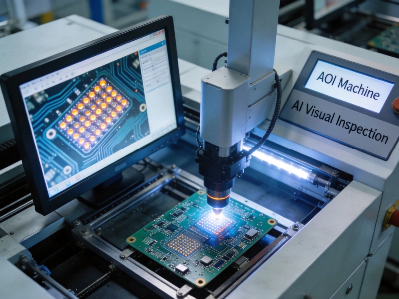
Inspection approaches differ significantly between the two processes. Reflow assemblies require Aoi for top-side visual inspection and X-ray for bottom-side and hidden joints. Wave soldering creates joints that are more accessible to visual inspection, though the speed of the process limits manual inspection opportunities. Automated Optical Inspection supplements visual checking for both processes, but the specific defect modes each produces require tailored inspection strategies.
Most modern electronic assemblies incorporate both surface mount and through-hole components, requiring manufacturing strategies that combine reflow and wave soldering processes. The sequence of these combined processes significantly impacts Assembly Quality, cost, and complexity. Planning for mixed-technology assembly must begin early in the design phase to ensure that components are selected and placed for optimal manufacturability.
The most common approach processes SMD components first through reflow, then adds through-hole components for wave soldering in a subsequent operation. This sequence protects temperature-sensitive SMDs from the higher thermal exposure of wave soldering while enabling efficient through-hole processing. However, this approach requires boards with SMDs only on the top side, limiting placement flexibility for some designs.
Double-sided reflow assemblies with bottom-side SMDs cannot use wave soldering for through-hole components, as the reflow processing for the second side would remelt joints from the first side. Selective soldering addresses this limitation by soldering through-hole components individually with localized heat application. While slower than wave soldering, selective solder systems offer flexibility for complex mixed-technology assemblies.
Design decisions significantly impact the manufacturability of mixed-technology assemblies. Placing all SMD components on the top side enables simple sequential processing: reflow for SMDs followed by wave for through-hole components. This single-sided SMD approach should be the default for designs incorporating both technologies unless space constraints or other factors require bottom-side placement.
Through-hole component placement affects wave soldering efficiency and defect rates. Components should be oriented to avoid shadowing, where tall components block solder from reaching shorter components behind them. Maintaining consistent spacing between through-hole components enables uniform flux application and solder contact. Design reviews with manufacturing engineers help identify placement issues before production begins.
Pad design for wave soldering differs from reflow pad specifications in several ways. Pads must provide adequate annular ring for reliable solder fill while avoiding excess size that could cause bridging. Solder mask dam design becomes critical for preventing solder creep or bridging between adjacent pads. Following manufacturer guidelines for pad geometry ensures optimal wave soldering results.
China's dominance in electronics manufacturing stems from decades of investment in manufacturing infrastructure, workforce development, and supply chain optimization. SMT assembly capabilities in China range from small operations with basic equipment to world-class facilities serving major international brands. This spectrum of capabilities enables Chinese manufacturers to serve diverse market segments cost-effectively.
Chinese SMT assembly facilities have adopted both wave and reflow technologies extensively, reflecting the global nature of the electronics industry they serve. High-volume Consumer Electronics production relies heavily on reflow technology for efficiency, while industrial and specialty electronics continue using wave soldering for through-hole components. The mix of equipment varies by manufacturer, with larger facilities typically maintaining both capabilities.
Labor costs in China, while rising, remain competitive compared to manufacturing in developed economies. However, the primary cost advantages derive from equipment utilization, supply chain integration, and manufacturing expertise developed through decades of specialization. Chinese manufacturers have achieved exceptional efficiency in SMT assembly, translating to competitive pricing for global customers.
Equipment quality and maintenance practices significantly impact the capabilities of Chinese SMT assembly partners. Modern reflow ovens with precise thermal profiling capabilities and nitrogen atmospheres distinguish advanced manufacturers from basic operations. Wave soldering equipment with continuous solder analysis and maintenance programs indicates commitment to quality rather than merely acceptable output.
Process control documentation and Traceability systems demonstrate manufacturing maturity. Facilities that maintain statistical process control data, thermal profiling records, and complete lot Traceability provide assurance of consistent quality. Quality management certifications including ISO 9001 and industry-specific standards such as Iatf 16949 for automotive applications indicate systematic quality approaches.
Engineering capabilities distinguish excellent manufacturing partners from mere assembly services. Partners who can advise on Design For Manufacturability, recommend component alternatives, and collaborate on problem-solving provide value beyond simple assembly. These engineering capabilities often prove more valuable than low pricing for complex or demanding applications.
Process costs for wave versus reflow soldering depend on equipment utilization, labor requirements, and material consumption. Reflow processing offers exceptional throughput once profiles are established, spreading setup costs across large production volumes. Wave soldering often has lower per-board costs for pure through-hole assemblies but requires separate assembly steps that add complexity.
Mixed-technology assemblies using sequential reflow and wave processing incur costs for both processes plus handling between operations. The complexity of mixed-process manufacturing often exceeds the sum of individual process costs due to additional setup requirements and potential yield impacts from multiple thermal cycles. Optimizing designs to minimize mixed-process requirements often reduces overall manufacturing costs.
Material costs vary between processes, with solder paste representing the primary material expense for reflow and solder consumption significant for wave processing. Flux costs, nitrogen consumption, and solder pot maintenance add to wave soldering material expenses. These material cost differences are typically modest compared to labor and overhead but should be considered in detailed cost analysis.
Production volume significantly influences the relative economics of wave and reflow processing. High-volume production favors reflow for its throughput advantages, with per-board costs decreasing sharply as volume increases. Wave soldering, while potentially offering lower per-board costs for suitable assemblies, may have higher setup costs that amortize less favorably across smaller volumes.
Low-volume production often benefits from selective soldering processes that eliminate wave soldering equipment setup requirements. While selective soldering is slower than wave, the elimination of dedicated wave setup makes it economical for small batches and prototypes. Many Chinese assembly partners offer flexible processing options that accommodate both high-volume and prototype quantities.
Product lifecycle considerations influence manufacturing strategy as well. Products in introduction or decline phases with lower volumes benefit from manufacturing approaches with lower setup requirements. Products in high-volume growth phases justify the setup investments that reflow efficiency rewards. Aligning manufacturing strategy with product lifecycle stages optimizes cost throughout the product journey.
Quality standards for SMT assembly in China vary widely among manufacturers, from basic commercial practices to certified quality management systems meeting international standards. Customers with demanding applications should verify that manufacturing partners hold appropriate certifications and can demonstrate systematic quality practices. The investment in quality verification protects against costly field failures and reputation damage.
Ipc Standards define industry consensus requirements for Electronics Assembly quality. Ipc-a-610 establishes acceptability criteria for electronic assemblies, providing objective standards for joint quality and component placement. Manufacturers certified to Ipc Standards demonstrate training and competency in industry best practices. Level 3 certification, the most stringent commercial standard, indicates capability for demanding applications.
Industry-specific certifications address requirements for specialized applications. Iatf 16949 for Automotive Electronics mandates specific process controls and documentation. AS9100 for aerospace applications requires additional quality provisions. Iso 13485 for medical devices imposes design controls and risk management requirements that affect Pcb Assembly. Customers in regulated industries should verify that partners hold relevant certifications.
Process validation demonstrates that manufacturing processes consistently produce acceptable results. For reflow soldering, validation includes thermal profiling across the board surface, confirming that all locations experience appropriate temperature profiles. For wave soldering, validation addresses flux application, solder temperature, and contact parameters. Documentation of validation results provides evidence of process capability.
Ongoing process monitoring maintains validated processes within acceptable variation limits. Statistical process control tracks key parameters including peak temperatures, conveyor speeds, and defect rates. Control charts identify trends that might indicate process drift before out-of-specification production occurs. Chinese manufacturers with robust SPC programs provide greater assurance of consistent quality.
First Article Inspection validates production readiness for new products or after significant changes. First articles undergo comprehensive examination including dimensional verification, Solder Joint Inspection, and functional testing when appropriate. Passing First Article Inspection confirms that processes are correctly configured and production can proceed. This gate prevents defective production runs from consuming resources and missing schedules.
SMT assembly technology continues evolving, with new methods expanding manufacturing possibilities and addressing limitations of traditional approaches. Laser soldering, vapor phase soldering, and advanced selective soldering systems offer capabilities that supplement conventional reflow and wave processes. Chinese manufacturers are adopting these emerging technologies to serve demanding applications that traditional methods cannot adequately address.
Miniaturization trends drive adoption of finer-pitch components, smaller packages, and higher-density assemblies. These trends challenge existing manufacturing capabilities and drive continuous equipment upgrades. Manufacturers investing in advanced placement systems, finer stencil capabilities, and improved process controls maintain competitiveness for leading-edge applications. Understanding a manufacturer's technology roadmap helps anticipate their ability to support evolving product requirements.
Lead-free solder transition, driven by environmental regulations, has largely completed in Chinese manufacturing. Lead-free alloys present different processing requirements than traditional tin-lead, with higher melting temperatures and different wetting characteristics. Chinese manufacturers have developed expertise in lead-free processing, though some applications may still benefit from traditional alloys where permissible.
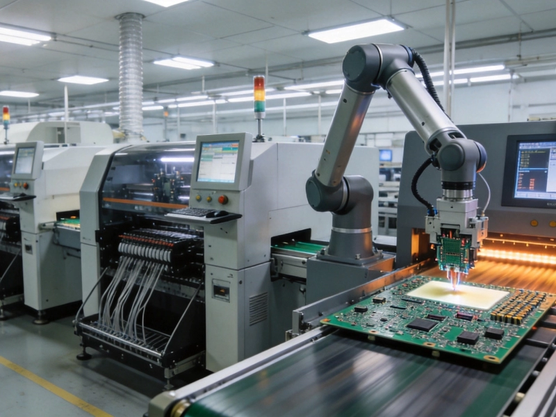
Manufacturing automation continues advancing in Chinese SMT facilities, reducing labor dependency while improving consistency. Automated material handling, vision-guided placement, and robotic inspection increase throughput while reducing human error. Facilities implementing Industry 4.0 concepts with connected equipment and data analytics achieve new levels of process optimization and predictive maintenance.
Machine learning and artificial intelligence increasingly contribute to quality improvement. Automated defect classification, predictive quality modeling, and process optimization algorithms identify issues before they manifest as defects. Chinese manufacturers at the technology frontier are implementing these capabilities, offering customers access to advanced quality improvement tools.
Environmental sustainability increasingly influences manufacturing practices. Energy-efficient equipment, waste reduction programs, and responsible material handling demonstrate commitment to sustainability. While these practices primarily benefit the environment, they often align with operational efficiency improvements that benefit customers through lower costs and more reliable supply chains.
Q: Can wave soldering damage surface mount components?
A: Yes, wave soldering can damage temperature-sensitive SMDs if they are on the bottom side of the board during wave processing. Standard practice is to place all SMDs on the top side and reserve the bottom side for through-hole components that will be wave soldered. If bottom-side SMDs are unavoidable, selective soldering or Hand Soldering must be used for through-hole components.
Q: Which process is better for high-volume production?
A: Reflow soldering generally offers better throughput for high-volume production, particularly for pure SMD assemblies. The ability to process all components simultaneously enables faster cycle times and lower per-board costs. Wave soldering can be cost-effective for high-volume through-hole assemblies but requires consideration of defect rates and quality control complexity.
Q: Can mixed SMD and through-hole boards use only one process?
A: Sometimes, if all SMDs are on the top side and through-hole components are limited. In this case, reflow first attaches SMDs, then wave soldering processes through-hole components. If SMDs exist on the bottom side, selective soldering must supplement reflow processing for through-hole components.
Q: What quality inspection is needed for reflow versus wave assemblies?
A: Reflow assemblies require Aoi for visual inspection and often X-ray for hidden joints from BGA or QFN packages. Wave soldering creates more visible joints but may require AOI for fine-pitch components. Both processes benefit from functional testing that verifies assembly operation beyond simple electrical continuity.
Q: How do I choose between wave and reflow capable manufacturers?
A: Evaluate based on your specific product requirements. Pure SMD assemblies need only reflow capability. Through-hole dominant assemblies may benefit from wave capability. Mixed-technology products need both capabilities or selective soldering. Consider equipment age, process controls, certifications, and engineering support in addition to basic capability.
Understanding the differences between wave soldering and reflow soldering is essential for successful SMT PCB Assembly, whether manufacturing in China or elsewhere. Each process offers distinct advantages suited to different applications, component types, and production volumes. Reflow soldering dominates for surface mount assemblies, providing throughput and consistency that enable cost-effective high-volume production. Wave soldering remains essential for through-hole components and assemblies requiring selective processing.
Chinese SMT assembly capabilities have matured to serve demanding applications across diverse industry segments. World-class facilities combine advanced equipment with systematic quality management and engineering expertise. Sourcing partners in China requires evaluating not just basic capabilities but the quality systems, process controls, and engineering support that ensure successful outcomes for specific applications.
The choice between wave and reflow soldering, or combinations of both, should be driven by technical requirements rather than manufacturing convenience. Designs optimized for manufacturability simplify process selection and improve quality outcomes. Collaboration between design engineers and manufacturing partners throughout development ensures that products are designed for the most appropriate manufacturing approach, reducing costs and improving time to market.
What to Expect During the First Article Inspection (FAI) of Your SMT PCB Assembly in ChinaSeptember/30/2026
The Importance of X-Ray Inspection for BGA in China's SMT Assembly ProcessAugust/03/2026
How China's SMT PCB Assembly Process Meets International IPC-A-610 StandardsJuly/22/2026
The Complete Process WalkthroughMay/29/2026
How to Place Fiducial Marks for Accurate SMT PCB Assembly in ChinaAugust/15/2026
The Role of Automated Optical Inspection (AOI) in China's SMT Assembly LinesJune/16/2026
Step-by-Step: From Solder Paste Printing to Final Testing in China SMT AssemblyJuly/13/2026
Understanding Reflow Soldering Profiles Used in SMT PCB Assembly ChinaJune/30/2026