Open Nav

High-power LED assemblies are thermally demanding. Each LED converts electrical energy to light, but a substantial portion becomes heat that must be removed from the junction to maintain efficiency and longevity. When Thermal Management is inadequate, LED junction temperature rises, light output degrades, color shifts, and lifetime collapses. In SMT production, thermal problems that show up in the field often have their roots in Pcb Design, component selection, or assembly process.
This article presents a real-world case from a China Smt Pcb Assembly factory. The customer was an LED lighting manufacturer experiencing field failures that traced back to thermal issues. The factory solved the problem through a systematic approach that included Pcb Design changes, Thermal Management improvements, and process optimization. The lessons apply to any LED Smt Assembly where thermal performance matters.
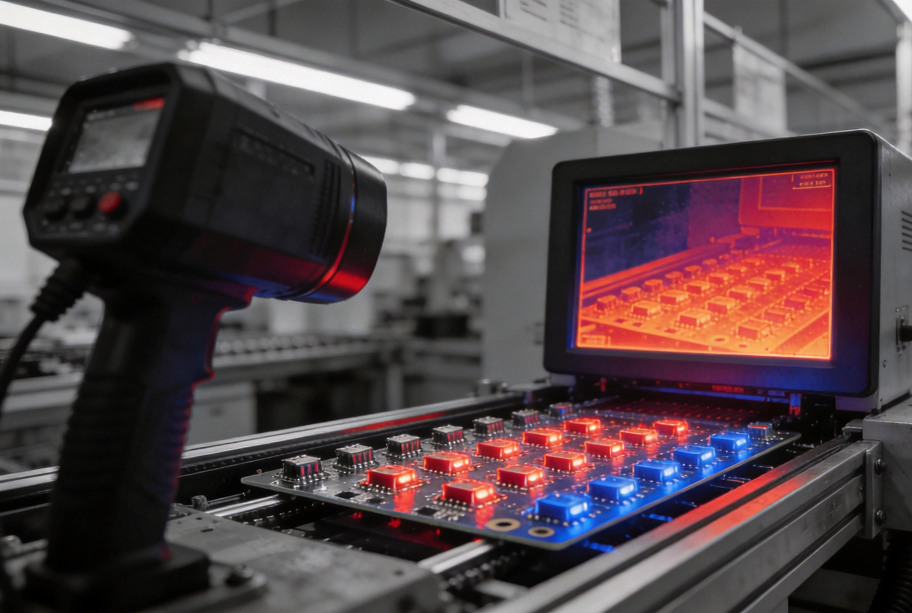
The customer designed a high-power LED lighting module using Smt Assembly in China. The specification called for 30,000 hours of operation at full drive current. In testing and early production, the boards met all performance criteria. But field returns started arriving after six months. The failure pattern was consistent — LED output had degraded by 20 to 30 percent, and some units had complete LED failures.
The customer requested root cause analysis. The factory brought in a cross-functional team including process engineers, PCB designers, and thermal analysis specialists. Their investigation revealed that LED junction temperature in the field was exceeding the rated maximum by 30 to 40 degrees Celsius under worst-case ambient conditions. The problem was not the LEDs themselves — it was the thermal path from junction to environment.
The investigation traced the thermal bottleneck through the assembly. Here is what they found.
The original design used a standard FR-4 substrate with 1 ounce copper. The thermal resistance of FR-4 is approximately 0.5 degrees Celsius per watt per mil. The LED thermal pad connected to a copper area on the top layer, but there was no direct thermal path to a bottom-side heat sink. Heat had to flow through the board thickness by conduction, which FR-4 does poorly.
The copper area under the LED thermal pad was insufficient. The pad was 3 millimeters by 3 millimeters, but the copper pour extended only 2 millimeters beyond the pad. For high-power LEDs, copper area directly under and around the thermal pad is critical for spreading heat before it enters the dielectric.
The design had no thermal vias under the LED thermal pads. Thermal vias — vias filled with conductive material that connect top-side copper to bottom-side copper — provide a low-resistance thermal path through the board. Without them, heat had to flow through the dielectric, which is the primary thermal bottleneck.
The assembly process used a standard solder paste stencil with 100 micron thickness. For the LED thermal pad, this resulted in insufficient solder thickness under the component. The solder joint provides a thermal path between the LED package and the PCB. Insufficient solder increases thermal resistance at this critical interface.
The factory was assembling the boards in a standard air-conditioned environment at 25 degrees Celsius. The actual operating environment for the lighting modules was industrial settings where ambient temperature could reach 50 degrees Celsius. The thermal design assumptions did not match the real-world operating conditions.
The solution involved changes at the PCB design level, the component level, and the assembly process level. No single change would have been sufficient.
The factory recommended a metal-core PCB (MCPCB) substrate instead of FR-4. MCPCB uses an aluminum or copper base plate with a thin dielectric layer and copper circuit layer on top. The thermal resistance of MCPCB is dramatically lower than FR-4 because the metal base plate conducts heat efficiently across the entire board.
For the specific application, they selected a 1.5 millimeter aluminum MCPCB with 35 micrometer copper circuit layer and 75 micrometer dielectric. This construction provided a thermal resistance of approximately 0.1 degrees Celsius per watt — five times better than the original FR-4 design.
The Pcb Layout was revised to increase the copper area under LED thermal pads. The copper pour was extended to 6 millimeters beyond each pad edge, creating a larger thermal spreading area. This change alone reduced junction temperature by 8 degrees Celsius in simulation.
The redesigned board included a thermal via array under each LED thermal pad. The pattern was 4 by 4 vias in a 0.5 millimeter grid, each via 0.3 millimeter diameter. The vias were filled with conductive epoxy to eliminate air gaps that would increase thermal resistance. The thermal vias provided a direct conduction path from the top-side copper to the aluminum base plate, bypassing the dielectric layer.
The customer and factory reviewed alternative LED packages. The original design used a surface-mount LED package with an exposed thermal pad on the bottom. They evaluated an alternative package with a larger thermal pad and a lower thermal resistance from junction to pad. The alternative package cost slightly more but provided 15 percent better thermal performance.
After thermal modeling, they determined that the MCPCB redesign with thermal vias provided sufficient improvement without changing the LED package. This decision kept component costs unchanged and avoided a major qualification effort.
The assembly process was updated to address the solder paste issue. A stepped stencil was designed with a thicker opening for LED thermal pads — 150 microns instead of 100 microns. This increased solder volume under the LEDs, improving the thermal interface.
The Reflow Profile was adjusted to ensure complete solder wetting on the large thermal pads without overheating the LEDs. LEDs are sensitive to peak reflow temperature. The profile was optimized with a lower peak temperature and extended time above liquidus to ensure adequate solder joint formation.
The final assembly included a thermal interface material between the MCPCB and the heat sink. The original design mounted the board directly to a heat sink with mechanical screws, which created air gaps at the interface. The revised design used a phase-change thermal pad that filled microscopic surface imperfections and provided a continuous thermal path.
The factory implemented the changes in a pilot production run. They conducted thermal validation to confirm the improvement.
Infrared thermal imaging measured LED surface temperature at full drive current in a controlled ambient temperature of 50 degrees Celsius. The original design showed LED surface temperatures of 85 degrees Celsius. The redesigned MCPCB with thermal vias and optimized assembly showed LED surface temperatures of 58 degrees Celsius — a 27-degree reduction.
Using the measured thermal resistance from junction to case provided by the LED manufacturer, the factory calculated junction temperature. The original design reached junction temperatures of 120 degrees Celsius, exceeding the rated maximum. The redesigned board maintained junction temperatures below 85 degrees Celsius, well within the specified operating range.
Accelerated life testing subjected the redesigned boards to elevated temperature and drive current to simulate 30,000 hours of operation in compressed time. The boards showed minimal light output degradation — less than 5 percent — and no LED failures through the test. This contrasted sharply with the 20 to 30 percent degradation seen in the original design after equivalent field exposure.
After validation, the factory implemented the changes in full production. Key aspects of the implementation:
The MCPCB fabrication process required supplier qualification. The factory worked with an MCPCB specialist in China to ensure consistent dielectric thickness and thermal performance. First-article inspection included cross-section analysis to verify dielectric thickness and thermal via fill quality.
The stepped stencil required process setup verification. The factory ran several test boards to confirm solder paste volume and Reflow Profile before releasing the design to production. Solder Joint Inspection verified that increased paste volume did not cause bridging or other defects.
Quality control added thermal measurement as a regular inspection step. A sample from each production lot is tested at full drive current to verify that thermal performance remains within specification.
This case illustrates several important lessons for LED SMT assembly thermal management.
The original design was adequate for 25-degree Celsius ambient but failed at 50-degree Celsius ambient. Thermal design must account for worst-case operating conditions, not laboratory conditions. For industrial or outdoor applications, this means higher ambient temperature assumptions.
FR-4 is the default PCB material, but it is not the right choice for high-power thermal applications. MCPCB or IMS substrates provide dramatically better thermal performance. The material choice has the largest impact on overall thermal resistance.
Adding thermal vias increases fabrication complexity and cost. However, the thermal benefit is substantial. For designs where thermal performance is critical, thermal vias are justified. The 4 by 4 via array used in this case added minimal cost but provided significant temperature reduction.
Solder paste volume and reflow profile are not just electrical and mechanical considerations — they affect thermal resistance. Insufficient solder under a thermal pad increases thermal resistance. The stepped stencil was a cost-effective solution that improved thermal performance without changing components or board material.
Testing at nominal conditions does not reveal thermal problems. Validation should include worst-case ambient temperature, maximum drive current, and any other stress conditions that the product will encounter in service. Thermal imaging and junction temperature calculation should be part of the qualification process for any LED assembly.
The thermal redesign added cost but far less than the cost of field failures. MCPCB substrate cost approximately 30 percent more than the original FR-4 board. The stepped stencil was a one-time tooling cost of approximately $200. The overall cost increase per board was approximately 15 percent.
Timeline impact was approximately six weeks for MCPCB supplier qualification, stencil fabrication, and process validation. This delay was acceptable because the alternative was continued field failures and reputational damage.
The principles from this case apply broadly to LED SMT assemblies. If you are designing or sourcing LED PCB assembly in China or elsewhere, consider these questions:
Does the PCB substrate match the thermal requirements? MCPCB is the right choice for high-power LED applications. FR-4 may be acceptable for low-power indicator LEDs but not for lighting modules.
Are thermal vias used under LED thermal pads? If not, consider adding them. The thermal benefit is significant relative to the added cost.
Does the solder paste volume provide adequate thermal interface? Review stencil design and reflow profile to ensure sufficient solder under thermal pads.
Does the thermal design account for worst-case operating conditions? Verify that junction temperature stays within specification at maximum ambient temperature and maximum drive current.
Has thermal validation been performed? Thermal imaging and junction temperature calculation should be part of qualification for any LED assembly where thermal performance affects lifetime or output.
Not always. For low-power indicator LEDs or very low-power lighting, FR-4 may be adequate. For high-power LED lighting modules, MCPCB is typically necessary to maintain acceptable junction temperature and lifetime. The decision depends on LED power dissipation, ambient temperature, and lifetime requirements.
The number of thermal vias depends on the LED power dissipation and the available board space. A 4 by 4 via array with 0.3 millimeter vias is a good starting point for medium-power LEDs. For very high-power LEDs, increase the via count and size. Simulations or thermal measurements can determine the optimal via pattern.
A larger heat sink helps, but if the thermal resistance from LED junction to heat sink is high, the heat sink cannot overcome the bottleneck. The PCB substrate and thermal path design are more fundamental. Improving the thermal path is usually more effective than oversizing the heat sink.
Measure LED case or surface temperature using thermal imaging or thermocouple. Use the thermal resistance from junction to case provided in the LED data sheet. Junction temperature equals case temperature plus the power dissipation multiplied by the thermal resistance from junction to case. This calculation provides an estimate that can be verified with more sophisticated methods if needed.
MCPCB thermal resistance is typically 0.05 to 0.15 degrees Celsius per watt depending on dielectric thickness and base plate material. FR-4 thermal resistance is typically 0.5 to 1.0 degrees Celsius per watt. MCPCB provides approximately five to ten times better thermal performance than FR-4 for the same thickness.
Tags: LED Thermal Management, SMT LED Assembly, MCPCB Design, Thermal Via Design, PCB Thermal Analysis, LED Junction Temperature, Thermal Imaging PCB, China SMT Assembly

Automotive Electronics Success: High-Reliability SMT PCB Assembly China Case StudyJuly/17/2026
Overcoming BGA Challenges in a Complex SMT PCB Assembly China ProjectJune/09/2026
Overcoming BGA Challenges in a Complex SMT PCB Assembly China ProjectMay/29/2026
How We Helped a US Startup Scale from Prototype to Mass SMT Assembly in ChinaJuly/07/2026

Industrial SMT PCB Assembly in China: Meeting Durability and Reliability StandardsJune/11/2026
The Role of Automated Optical Inspection (AOI) in China's SMT Assembly LinesJune/16/2026
Thermal Management in PCB Design: Preventing Warpage in China's SMT AssemblyJuly/15/2026
Understanding Reflow Soldering Profiles Used in SMT PCB Assembly ChinaJune/30/2026