
You receive your first production shipment from a Contract Manufacturer in Shenzhen. The boards look perfect—until you run them through reflow and watch them twist like potato chips cooling on a counter. The warpage exceeds tolerances. Components are misaligned. The entire order becomes scrap.
This scenario plays out regularly in China's Electronics Manufacturing ecosystem. Thermal warpage during Smt Assembly remains one of the most persistent quality challenges, especially as boards grow larger, thinner, and more densely populated with heat-sensitive components. Understanding Thermal Management isn't optional—it's the difference between production success and expensive failure.
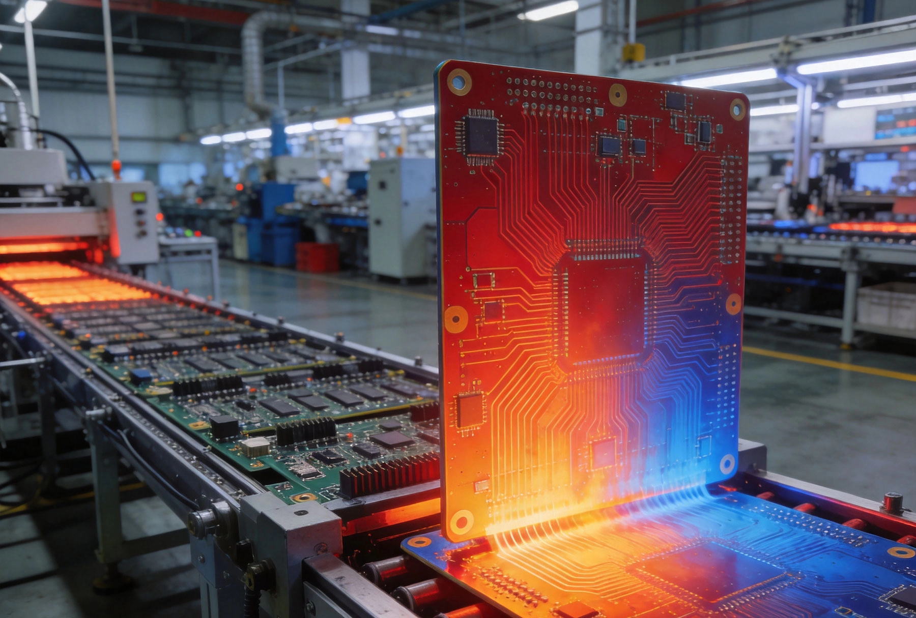
PCB warpage doesn't happen randomly. It follows predictable physics rooted in thermal expansion mismatches and stress accumulation during manufacturing processes.
Every material expands when heated and contracts when cooled. The rate of this expansion—measured as Coefficient of Thermal Expansion (CTE)—differs between the various materials in a PCB. Copper expands at roughly 17 ppm/°C. FR-4 laminate expands at 14-18 ppm/°C in the X-Y plane but much more—50-70 ppm/°C—in the Z-axis. Prepreg and core materials have their own CTE values that interact with copper during thermal cycles.
These mismatched expansion rates create internal stress. When stress exceeds the materials' limits, the board deforms. The deformation pattern depends on the symmetry—or asymmetry—of the board construction.
Certain board features concentrate thermal stress:
PCB substrate materials have a glass transition temperature (Tg) where the material transforms from rigid to rubbery. Below Tg, the material is stiff. Above Tg, it softens dramatically and CTE increases significantly.
Standard FR-4 has Tg around 130-140°C. High-Tg materials reach 170-180°C. When assembly peak temperatures approach or exceed Tg, the board softens and is more susceptible to deformation. Understanding your materials' Tg—and ensuring assembly profiles don't exceed it—is fundamental to warpage control.
Preventing warpage starts at the design phase. Board construction choices made during layout directly impact thermal behavior during assembly.
The single most effective warpage prevention technique is symmetrical construction. If your board has 6 layers, the stack-up should be symmetric around the neutral axis: layers 1-2-3 should mirror layers 6-5-4 in thickness and copper coverage.
Asymmetry creates differential stress during thermal cycles. One side expands more than the other, causing the board to bow toward the lower-expansion side. Symmetric stack-ups balance these forces and resist deformation.
Within each layer, copper distribution should be as uniform as practical. However, signal routing rarely achieves perfect balance. When imbalances are unavoidable:
Many designers specify "copper thieving"—dummy copper patterns—in low-density areas to improve balance without affecting electrical performance.
Production panels typically contain multiple board units. Array design significantly affects warpage behavior:
Tab-routed arrays maintain panel integrity during processing, reducing individual board warpage until depanelization. However, stress concentration at tabs can cause issues.
V-score panels allow more freedom between units but may experience unit-level warpage earlier in the process.
Mouse-bite arrays provide intermediate behavior but require careful breakout force control during depanelization.
Discuss array design with your CM—they often have preferences based on their specific equipment and process capabilities.
Material choice affects warpage susceptibility throughout the product lifecycle.
Match material Tg to your assembly thermal profile:
Materials with Tg close to assembly peak temperature are most susceptible to warpage. Always specify materials with comfortable margin above your peak process temperature.
Thicker boards resist warpage better than thin boards. When thickness reduction is necessary for form factor reasons, compensate through:
Boards thinner than 0.8mm for larger formats need particular attention. Some applications require 1.0mm or thicker for acceptable thermal stability.
Even within the same material type, different prepreg styles have different flow characteristics. During lamination, prepreg flows and fills voids. This flow affects final thickness and stress distribution.
Work with your manufacturer to specify prepreg types they stock and process consistently. Switching materials for cost reasons can introduce unexpected warpage issues.
Surface finish processes apply additional thermal cycles to completed boards—and can cause or exacerbate warpage.
Hot Air Solder Leveling applies significant thermal stress. The board dips into molten solder at 260-280°C, then experiences rapid air knife cooling. This thermal shock can induce warpage, especially in asymmetric constructions.
For warpage-sensitive applications, consider alternative finishes that apply less thermal stress:
ENIG applies nickel (290°C bath) then gold (80°C bath) in sequence. The nickel immersion process creates thermal stress that can affect warpage. Multiple ENIG processing passes (for rework or repair) compound this stress.
For tight warpage requirements, specify single-pass ENIG and avoid reprocessing.
Even well-designed boards can warp if assembly processes are aggressive. Profile optimization prevents unnecessary thermal stress.
The preheat zone serves multiple purposes: activating flux, reducing thermal shock, and evaporating volatiles. A well-designed preheat ramp:
Rapid preheat ramps create temperature gradients across the panel. Gradients mean differential expansion, which means stress, which means warpage.
Ramp-to-spike profiles heat boards continuously to peak temperature. These work for robust assemblies but can stress warpage-sensitive boards.
Ramp-soak-ramp profiles include a soak period (typically 60-120 seconds) at intermediate temperature before final ramp to peak. The soak allows temperature equalization across the panel, reducing gradients and associated stress.
For warpage-prone boards, soak periods reduce peak temperature gradients by 30-50% compared to ramp-to-spike approaches.
Cooling matters as much as heating. Rapid quench cooling after reflow introduces thermal shock that can warp boards or stress components. Controlled cooling—at 3-6°C per second—maintains stress within acceptable limits.
Some manufacturers use forced-air cooling systems rather than natural convection cooling. These systems provide consistent, controllable cooling rates but require calibration to avoid over-aggressive cooling.
Boards often pass through multiple reflow cycles: initial SMT paste printing, through-hole insertion reflow, Conformal Coating curing, and rework. Each cycle adds cumulative thermal stress.
Design for minimum reflow passes. When multiple passes are unavoidable:
Detecting warpage before assembly prevents downstream problems. Modern inspection techniques provide quantitative data.
Several techniques measure board flatness:
Shadow moiré projects patterns onto boards and analyzes distortion to calculate warpage with high precision. This non-contact method works on populated or unpopulated boards.
Contact profilometry physically traces the board surface with a probe. More accurate for absolute measurements but slower and requires board contact.
Laser scanning provides rapid surface mapping. Many modern Aoi systems include warpage measurement capabilities.
Specify measurement method and acceptance criteria in your procurement documentation. Typical warpage limits range from 0.5% to 1.5% depending on component sensitivity.
Measure flatness at multiple stages:
Tracking warpage progression through processes identifies which operations cause problems.
China's Electronics Manufacturing industry has specific capabilities and practices that affect warpage management.
Warpage requirements are meaningless if not communicated clearly. Specify:
Chinese CMs often appreciate quantitative requirements with clear acceptance criteria. Ambiguous specifications lead to ambiguous results.
Chinese manufacturers often source materials from multiple suppliers based on availability and pricing. While this flexibility benefits cost management, it can introduce variability.
For warpage-sensitive applications, specify approved material sources or require notification before material substitution. This prevents surprises when boards arrive with different material than qualification samples.
Ask potential CMs for process capability studies showing warpage data across their production. Key metrics include:
A Cpk above 1.33 indicates a capable process. Lower values suggest potential warpage control issues.
For new products or new CM relationships, First Article Inspection is essential. Request:
First article approval should be a prerequisite for production release. Boards that warp on first articles will warp in production.
Rework introduces additional thermal cycles to already-assembled boards—and can create warpage in boards that were initially flat.
Hot air rework stations can apply localized heat that causes board distortion if not controlled:
Bga Rework requires complete reflow of the component area—typically 230-260°C peak. This localized thermal exposure can induce warpage, especially on thin boards.
Consider board thickness and construction when specifying rework procedures. Some warpage-tolerant designs become warpage-prone after multiple reworks.
For severely warped boards, rework may not be economical. Establish clear criteria for rework vs. scrap decisions. Boards that exceed warpage tolerance after rework attempts should be scrapped rather than continued—continued processing wastes additional labor and materials.
Real-world warpage issues illuminate prevention strategies.
A 12-layer server board exceeded warpage limits after reflow. Investigation revealed:
Resolution: Redesigned layer distribution for symmetry, changed profile to 2°C/second with 90-second soak, reduced peak temperature by 5°C. Warpage reduced from 1.8% to 0.6%.
A 0.6mm thick medical board warped during ENIG processing. Root cause: multiple ENIG cycles with no stress relief between.
Resolution: Single-pass ENIG specified, incoming warpage inspection added, boards supported on ceramic backing plates during processing. Warpage reduced from 1.2% to 0.4%.
A board using both standard FR-4 and high-TG materials warped asymmetrically due to differential CTE between materials.
Resolution: Unified to single material system throughout stack-up, redesigned for full material compatibility. Asymmetric warpage eliminated.
Warpage prevention has costs—but uncontrolled warpage costs more.
Prevention investment typically costs 5-10% of failure costs. The return on investment is clear when failure costs are calculated honestly.
Thermal warpage in Pcb Assembly isn't mysterious—it follows predictable physics and responds to systematic prevention. The path to warp-free boards runs through design choices that create balanced, symmetric constructions; material selections matched to assembly thermal demands; and process profiles that minimize unnecessary stress.
Working effectively with Chinese Contract Manufacturers requires clear communication of requirements, understanding of their capabilities, and partnership in Continuous Improvement. Warpage isn't anyone's fault—it's a consequence of choices made throughout design and production. Systematic approach to those choices eliminates the problem.
As boards continue trending toward larger formats, thinner profiles, and more aggressive assembly profiles, warpage management becomes more important, not less. Building these capabilities now prepares you for the next generation of PCB challenges.
Component pitch determines requirements. Fine-pitch components (0.5mm and below) typically require 0.5% or less warpage. Standard components (0.65mm and above) tolerate 0.75-1.0%. BGA components need especially tight control. Discuss your specific components with your CM to establish appropriate limits.
Yes, significantly. Thinner boards are more susceptible to warpage than thicker boards of the same construction. Reducing board thickness by 50% can increase warpage by 200-300%. When thickness reduction is necessary, compensate with higher-Tg materials or reinforced construction.
Minor warpage (below 0.5%) can sometimes be corrected through controlled reheating and flattening. Severe warpage typically cannot be corrected without damaging the board. Prevention is far more reliable than correction.
Request statistical process data showing warpage measurements across multiple production runs. Cpk values above 1.33 indicate capable processes. Also request qualification data for boards similar to your upcoming production in size and thickness.
Conformal Coating adds a layer that may have different CTE than the board substrate. If applied after assembly, coating thermal cure cycles can induce additional warpage. Test warpage both before and after coating to verify acceptable results.
Bowing describes uniform curvature across the board—shaped like a potato chip. Warpage is more severe deformation involving twisting or irregular patterns. Both cause assembly problems, but warpage typically indicates more serious construction or process issues.
This article is intended for informational purposes. Consult with qualified Pcb Design engineers and experienced contract manufacturers for specific application guidance.
Avoiding Tombstoning: PCB Design Tips for Passive SMT Components in China AssemblyOctober/10/2026
How to Design the Perfect Land Pattern for SMT Components in Chinese FactoriesJune/18/2026
PCB Design Best Practices for High-Quality SMT Assembly in ChinaMay/29/2026
The Impact of PCB Surface Finish on SMT Assembly Soldering Quality in ChinaAugust/06/2026
Designing for Miniaturization: 0201 and 01005 Components in China SMT AssemblyJuly/26/2026
Designing Mixed-Technology Boards: Integrating THT and SMT Assembly for China ProductionSeptember/09/2026
PCB Stack-up Considerations for Reliable SMT PCB Assembly in Chinese Supply ChainsSeptember/20/2026
PCB Design Best Practices for High-Quality SMT Assembly in ChinaJune/05/2026