Open Nav
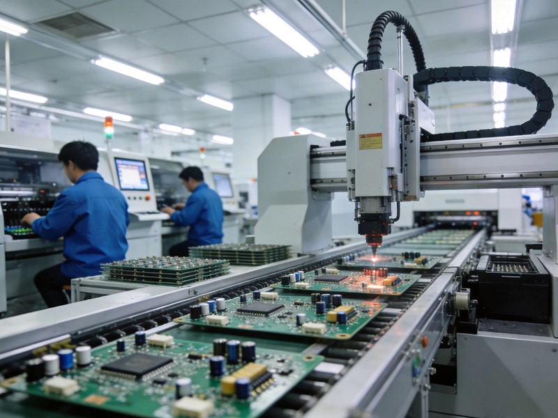
When it comes to Smt Pcb Assembly in China, the difference between a profitable product and a costly failure often comes down to one critical practice: Design for Manufacturability (Dfm) analysis. Yet many companies still wait until production has begun to discover design flaws that could have been caught—and corrected—weeks earlier.
Early Dfm analysis isn't just a best practice; it's one of the most powerful cost-reduction strategies available to electronics manufacturers. By identifying potential manufacturing issues during the design phase, companies can avoid expensive rework, production delays, and material waste that quietly erode profit margins on every PCB project.

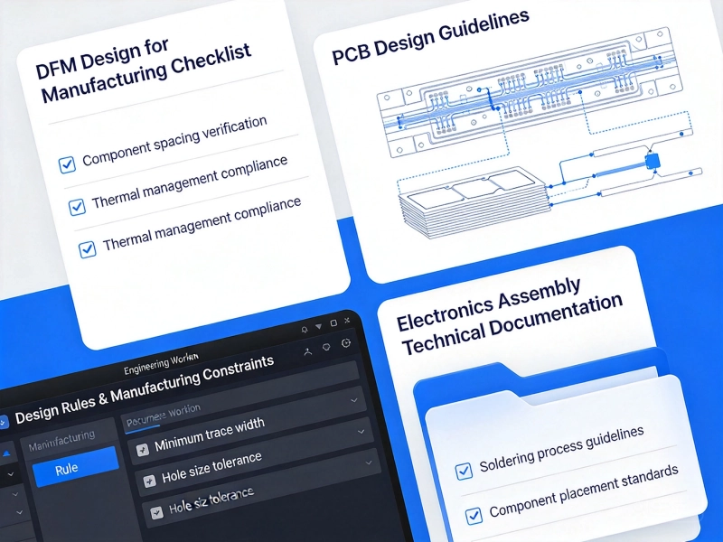
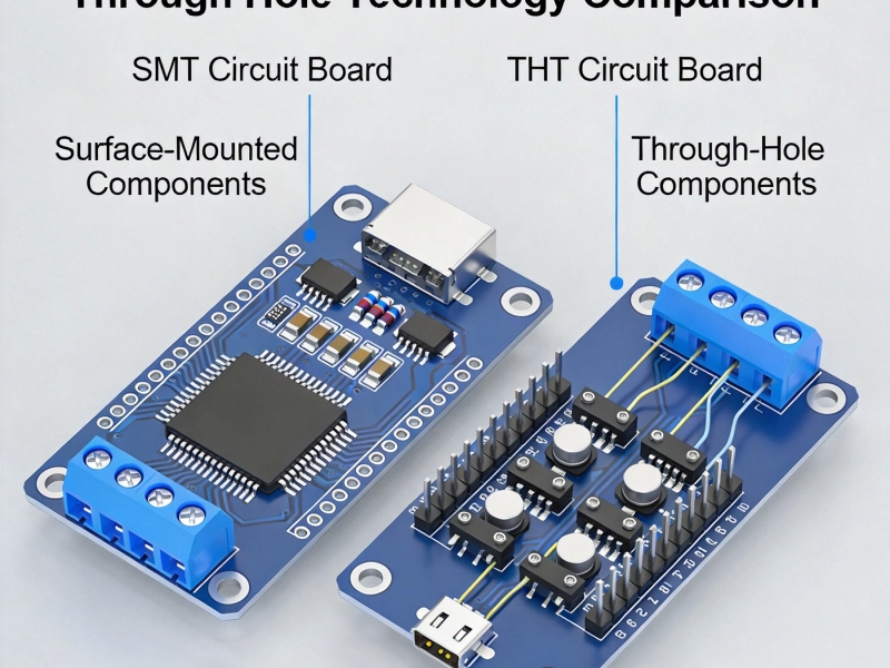
DFM analysis is the process of evaluating a Pcb Design for its compatibility with manufacturing processes before production begins. In the context of SMT (Surface Mount Technology) assembly, this means reviewing component placement, pad geometries, solder joint reliability, and panelization strategy to ensure the design can be efficiently produced at scale.
China's contract manufacturers have invested heavily in advanced DFM capabilities precisely because they understand the economics. A design flaw discovered during production might require:
These costs multiply quickly. Early DFM analysis catches 70-80% of these issues before a single board is assembled, transforming potential disasters into manageable design tweaks.
The first PCB prototypes often reveal design issues that require multiple revision cycles. Each iteration adds engineering labor costs, tooling modifications, and time delays. By conducting thorough DFM analysis early—ideally during schematic capture or initial layout—design teams can reduce NPI cycles from 4-5 iterations down to 1-2, cutting thousands of dollars in development expenses.
Chinese SMT factories price PCB assembly partly based on panel efficiency. A poorly designed PCB that yields 60% panel utilization will cost significantly more per board than an optimized design achieving 85-90% utilization. DFM analysis reviews:
Component selection has massive cost implications. DFM analysis examines:
Many designers specify components that are technically suitable but economically inefficient. A skilled DFM review often identifies 15-25% component cost reduction opportunities without compromising performance.
When boards fail inspection—whether due to tombstoning, bridged solder joints, or misaligned components—the factory must either rework each affected board or scrap it entirely. Rework labor alone typically costs $5-25 per board, while scrapped boards represent 100% material loss. Early DFM analysis prevents these failures by ensuring:
The spatial arrangement of components directly affects assembly speed and defect rates. During DFM review, engineers examine:
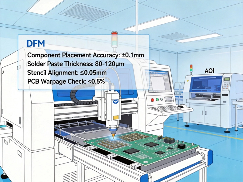
Pad geometry is where many designs fail. Even slight deviations from recommended specifications can cause field failures that damage brand reputation and trigger costly warranty claims. Critical pad-related DFM checks include:
Assembly efficiency depends on design choices that affect how easily boards flow through production. DFM analysis evaluates:
The best time to involve your Chinese contract manufacturer is during the schematic design phase, before any Pcb Layout work begins. Share your product requirements, target volumes, and cost objectives. Experienced CM engineers can suggest component alternatives, board layer count decisions, and impedance requirements that impact both performance and cost.
Before releasing files for production, request a formal DFM analysis report from your manufacturer. This report should include:
DFM isn't a one-time activity. Establish a review cadence that includes:
To justify the time investment, measure the financial impact of DFM analysis. Track metrics like:
While via-in-pad can reduce board size, improperly designed via-in-pad configurations cause solder wicking, voiding, and reliability failures. DFM analysis ensures proper tenting, filling, or capping based on the assembly requirements.
_h3>Fine-Pitch Component RegistrationComponents with 0.4mm or smaller pitch require extremely precise paste registration and placement accuracy. A DFM review verifies that the manufacturer's equipment can meet these tolerances and that the design includes appropriate tooling enhancements if needed.
High-power components often have conflicting thermal requirements. Some need thermal pads connected to planes for heat dissipation; others need isolation to prevent heat damage. DFM analysis identifies these conflicts before they cause field failures or production delays.
Silkscreen errors—missing, obscured, or incorrect component designators—cause assembly mistakes that require costly rework. DFM review verifies silkscreen legibility and placement relative to component bodies.
Not all Chinese SMT factories offer the same level of DFM support. When evaluating potential partners, consider:
Many Western companies find that the initial investment in relationship-building with a Chinese CM—including collaborative DFM sessions—pays dividends for years through consistently lower costs and smoother production ramps.
In an industry where margins are constantly squeezed, early DFM analysis stands out as a strategy that benefits everyone: designers get better products, manufacturers run more efficiently, and end customers receive more reliable electronics at lower prices.
Companies that make DFM analysis a standard practice—rather than an optional add-on—consistently outperform competitors on cost, quality, and time-to-market. The question isn't whether your organization can afford to invest in early DFM analysis; it's whether you can afford not to.
DFM analysis should begin during the schematic design phase, before any layout work starts. This allows design decisions to incorporate manufacturing constraints from the beginning, rather than requiring costly redesigns later. Initial concept reviews with your CM can be completed in 1-2 hours and prevent weeks of wasted effort.
For a standard multilayer PCB (4-8 layers), a thorough DFM review usually takes 2-5 business days, depending on the complexity and the CM's current workload. For highly complex designs with fine-pitch components or advanced requirements, allow 7-10 days for a detailed analysis.
Provide your CM with Gerber files (RS-274X format), NC drill files, the bill of materials (BOM), pick-and-place files, and any stackup or impedance requirements. The more complete the information package, the more accurate the DFM analysis will be.
While DFM review requires additional time upfront (typically 2-5 days), it dramatically reduces total project time by preventing production delays, multiple prototype iterations, and potential product launch failures. Most projects see a net timeline improvement of 20-30%.
Savings vary by project complexity, but industry data suggests typical cost reductions of 15-30% on complex assemblies through a combination of fewer prototype iterations, reduced rework rates, optimized component selection, and improved production efficiency. For high-volume products, these savings can represent hundreds of thousands of dollars over the product lifecycle.
Ready to optimize your next PCB project for cost and manufacturability? Contact our engineering team to discuss how early DFM analysis can reduce your Smt Assembly costs while improving product quality and time-to-market.
Essential DFM Guidelines for SMT PCB Assembly in ChinaMay/29/2026
Essential DFM Guidelines for SMT PCB Assembly in ChinaJune/04/2026
Which Technology is Right for Your Project?May/29/2026

Top Applications of SMT PCB Assembly in China: From Automotive to IoTJune/15/2026
How to Get Quick-turn SMT PCB Assembly in Just 24 Hours from ChinaJune/12/2026
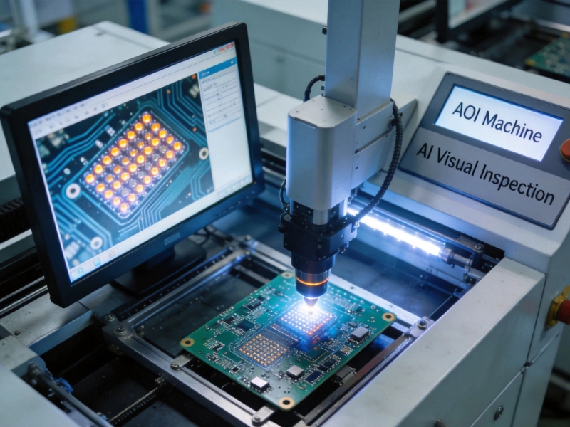
The Role of Automated Optical Inspection (AOI) in China's SMT Assembly LinesJune/16/2026

How to Get Quick-turn SMT PCB Assembly in Just 24 Hours from ChinaMay/29/2026
The Complete Process WalkthroughMay/29/2026