Open Nav
When you partner with electronics manufacturers in China, getting your land pattern designs right isn't just a technical detail—it's the difference between smooth production runs and costly respins. Your PCB footprint directly impacts solder joint reliability, assembly yield rates, and long-term product durability. Most engineers know the basics, but the nuances that separate adequate designs from manufacturing-optimized ones often get overlooked until problems surface on the production line.
This comprehensive guide walks you through everything you need to know about designing SMT land patterns that Chinese factories can produce efficiently and reliably. Whether you're working with a small Shenzhen assembly house or a large-scale OEM facility, these principles apply across China's diverse electronics manufacturing landscape.

A land pattern—also called a footprint or pad pattern—serves as the connection interface between your SMT component and the PCB. It consists of exposed copper pads where solder paste gets applied and the component leads get placed. The geometry of these pads, their spacing, and their relationship to the component termination all critically affect the manufacturing process.
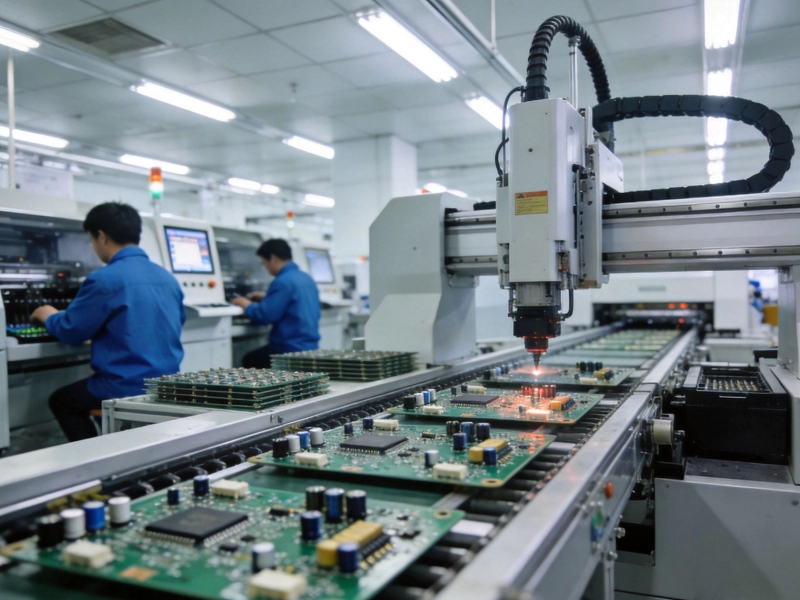
Chinese electronics factories operate at scales and speeds that demand precision from design stage. A typical assembly line in Shenzhen or Shanghai runs at pick-and-place speeds that leave no room for ambiguity in your footprint definitions. Every dimension, tolerance, and specification you provide must be crystal clear to avoid miscommunications that compound across thousands of units.
The three primary functions of a land pattern are mechanical retention, electrical connectivity, and Thermal Management. Get any of these wrong and you introduce risk into your product. The challenge lies in balancing all three while maintaining compatibility with standard manufacturing processes used across Chinese facilities.
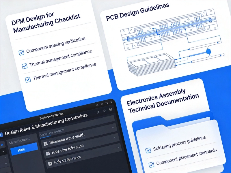
Almost every reputable electronics manufacturer in China follows IPC guidelines for land pattern design. The IPC-7351 standard defines nominal land pattern geometries for surface mount packages, and your Chinese partners expect your footprints to align with these specifications. Understanding this standard isn't optional—it's foundational.
IPC-7351 introduces the concept of density levels: Density Level A (most conservative), Density Level B (nominal), and Density Level C (most dense). Chinese factories typically work at Density Level B, but many high-volume consumer electronics manufacturers push toward Level C for cost optimization. You need to know which density level your specific factory partner uses and design accordingly.
When you submit documentation to Chinese factories, always specify which IPC density level your land patterns target. If you don't specify, they'll often default to Level B—which might be too conservative for space-constrained designs or too aggressive for high-reliability applications. This single specification prevents countless back-and-forth clarifications during production planning.
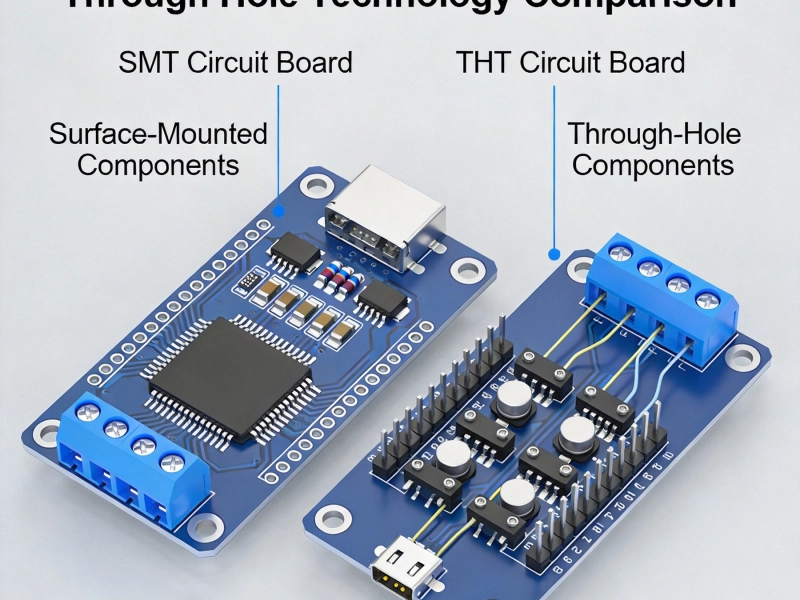
Different package types demand different land pattern approaches. Resistors and capacitors (0201, 0402, 0603, 0805, 1206) represent the most common components in Chinese factories. The rule of thumb for these passive components: extend your pad beyond the component termination by about 0.3mm to 0.5mm on each side, depending on the density level you target.
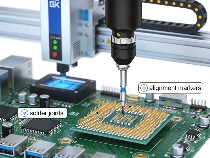
For ICs with gull-wing leads (SOIC, TSSOP, QFP), the toe fillet extension becomes critical. Your land pattern must provide enough solder volume to create reliable fillets without causing bridging. Chinese assembly houses typically expect toe projections of 0.1mm to 0.25mm beyond the component lead tip. Getting this wrong in either direction creates problems—too little risks insufficient solder joint strength, too much increases bridging risk.
Ball Grid Array (BGA) packages present unique challenges in Chinese factories. The solder ball collapse during reflow must be calculated precisely. For standard BGAs, plan for approximately 0.2mm to 0.3mm collapse during the reflow process. Your land pattern diameter should account for this collapse while maintaining proper self-centering forces. Many Chinese factories have extensive experience with BGAs, but clear documentation of your expected paste aperture and land diameter tolerances prevents surprises.
Power components and thermal-critical designs require extra attention when manufacturing in China. Thermal pads underneath packages like QFN, Power MOSFETs, and voltage regulators demand specific treatment. These thermal pads serve dual purposes: electrical connection for the center pad and heat dissipation to the PCB.
For thermal pads, Chinese factories expect you to specify both the land pattern dimensions and the thermal via configuration. Standard practice includes thermal vias on 1.0mm to 1.2mm pitch beneath the thermal pad. These vias should be either tented (covered with solder mask) or plugged (filled with non-conductive material) depending on your reliability requirements. Tented vias reduce solder wicking but may trap air during reflow; plugged vias provide more consistent thermal performance.
Thermal relief patterns connect your thermal pad to the surrounding copper plane. Your Chinese factory expects you to specify the spoke width and number of thermal spokes—typically 4 to 8 spokes of 0.2mm to 0.3mm width. This connection strategy balances mechanical stability with controlled thermal conductivity. Too many spokes or too wide a connection creates solder drain problems; too few compromises thermal performance.
Your land pattern design only performs as well as the solder paste application supporting it. In Chinese factories, stencil thickness and aperture design directly determine paste volume. For standard SMT components, stencil thicknesses of 0.1mm to 0.15mm are common, with 0.12mm representing a popular middle ground.
Stencil aperture design typically follows the land pattern with some reduction. For most components, apertures should be approximately 80% to 90% of the land pattern area. This reduction prevents solder balling and bridging while still providing sufficient volume for reliable joints. Your Chinese manufacturing partner may have standard aperture reduction percentages they apply automatically, but providing your preferred specification gives you better control.
For fine-pitch components (0.4mm pitch and finer), aperture design becomes even more critical. Chinese factories with advanced capabilities use laser-cut stencils with micro-apertures for these delicate applications. Specify your paste volume requirements explicitly and ask your factory to confirm their stencil manufacturing capability matches your pitch requirements. The cost difference between standard and laser-cut stencils is minimal compared to yield losses from paste-related defects.
Design For Manufacturability (Dfm) in Chinese factories means accounting for real-world tolerances. Your component tolerances, PCB fabrication tolerances, and assembly tolerances all stack. Understanding how these tolerances combine helps you set realistic land pattern specifications that your Chinese partners can consistently achieve.
PCB fabrication tolerances in China typically run ±0.1mm for standard tolerance boards and tighter for premium classes. Your land pattern dimensions should accommodate this variation while maintaining minimum annular ring requirements. When you specify land pattern dimensions, always include tolerance ranges rather than just nominal values. A land pattern specified as "1.5mm × 1.0mm" leaves too much ambiguity; "1.5mm ± 0.1mm × 1.0mm ± 0.1mm" communicates your actual requirements clearly.
Component placement accuracy in modern Chinese factories is excellent—typically ±0.05mm for standard placement equipment. However, component lead coplanarity variations and PCB warpage can introduce placement-related issues. Your land pattern design should provide adequate tolerance for these real-world conditions. Generous pad overlap (the area where the component lead sits on the pad) prevents tombstoning and improves first-pass yield.
The most common land pattern problems we see in Chinese manufacturing stem from documentation ambiguity. Your Chinese factory needs clear, unambiguous specifications. Gerber files with complete drill data, solder mask expansion specifications, and paste layer definitions form the minimum documentation package. Beyond these basics, providing a dimensioned drawing of critical land patterns prevents misinterpretation.
When communicating with your Chinese manufacturing partner, language clarity matters. Technical terms sometimes get lost in translation. Always provide both visual indicators (dimensioned drawings, callouts) and explicit numeric specifications. If you have preferred values for paste coverage percentage, paste mask thickness, or any other process parameters, state them explicitly rather than assuming your factory will use "standard" values.
Most Chinese factories have engineering teams experienced with international standards. They can often catch land pattern issues before production if you give them the opportunity. Share your design intent, expected operating environment, and reliability requirements. A factory that understands why you specified a particular land pattern can make intelligent suggestions when your design might cause manufacturing challenges.
Through years of supporting designs manufactured in China, certain patterns of land pattern errors repeatedly surface. One of the most frequent: using datasheet-recommended land patterns without adjusting for the specific manufacturing process your Chinese partner uses. Datasheet land patterns often target laboratory conditions, not high-speed production environments.
Another common mistake involves insufficient documentation of silkscreen and solder mask layers. Chinese factories need clear silkscreen markings to identify components correctly. If your silkscreen layer doesn't clearly label polarity, pin 1 indicators, or component references, assembly confusion follows. Similarly, solder mask expansion around land patterns affects paste deposition and must be specified consistently.
Testing and qualification reveals land pattern issues that simulation doesn't catch. Before committing to full production, request first article inspection from your Chinese factory. This first-run sample review catches land pattern issues while changes remain affordable. Many engineers skip this step to save time, only to discover systematic problems after thousands of units have already shipped.
Chinese factories excel at cost optimization, but land pattern corner-cutting creates long-term problems. The most reliable approach: design for robust manufacturing first, then optimize based on actual production data. Your initial land pattern design should prioritize first-pass yield and solder joint reliability. Once you have production data confirming stable processes, you can evaluate targeted optimizations.
Panelization affects land pattern design decisions. Chinese factories typically panelize boards in arrays for maximum efficiency. Your land patterns near panel edges need additional clearance for routing and depaneling. The stress induced during depanelization— whether by v-score, tab-route, or punch—can crack solder joints on land patterns too close to panel edges. Include depaneling clearance specifications in your design rules.
Quality verification costs money but pays dividends. X-ray inspection for BGA and QFN packages, cross-section analysis for critical joints, and thermal cycling testing for reliability validation all require investment. Work with your Chinese factory to establish appropriate quality verification protocols based on your product's application and reliability requirements. The cost of thorough qualification is always less than field failures and returns.
Designing land patterns for SMT components in Chinese factories requires balancing technical precision with practical manufacturing considerations. Start with IPC standards as your baseline, account for real-world tolerances, and always maintain clear communication with your manufacturing partners. The factories in China have decades of experience optimizing for efficiency— work with that expertise rather than around it.
Your land pattern specifications translate directly into manufacturing success or headaches. Invest the time to get them right, verify through first article inspection, and document thoroughly. These practices separate professional designs that ship smoothly from projects that languish in manufacturing problem-solving. When your land patterns are right, everything else in your manufacturing relationship becomes easier.
Partner with factories that ask questions about your land pattern specifications rather than assuming everything is standard. Their engineering engagement signals manufacturing maturity and genuine partnership capability. With the right approach to land pattern design, your Chinese manufacturing relationship becomes a competitive advantage rather than a technical risk to manage.

PCB Design Best Practices for High-Quality SMT Assembly in ChinaJune/05/2026

PCB Design Best Practices for High-Quality SMT Assembly in ChinaMay/29/2026

Top Applications of SMT PCB Assembly in China: From Automotive to IoTJune/15/2026

How to Reduce SMT PCB Assembly Costs in China with Early DFM AnalysisJune/17/2026
Essential DFM Guidelines for SMT PCB Assembly in ChinaMay/29/2026
Overcoming BGA Challenges in a Complex SMT PCB Assembly China ProjectJune/09/2026
Which Technology is Right for Your Project?May/29/2026
How to Get Quick-turn SMT PCB Assembly in Just 24 Hours from ChinaJune/12/2026