In our 15 years of operating SMT lines in Shenzhen and Suzhou, we've seen countless designs arrive at the factory floor that look perfect on CAD—but fall apart during production. Boards with components placed too close for robotic assembly. Pads sized incorrectly for paste printing. Thermal profiles that cause warpage on lead-free boards. These aren't edge cases; they're daily realities when design engineers lack visibility into manufacturing constraints.
Design For Manufacturability (Dfm) bridges the gap between what engineers design and what factories can actually produce consistently at scale. For PCB assemblies destined for China-based Smt Manufacturing, understanding local production capabilities, equipment specifications, and process limitations isn't optional—it's essential for controlling costs and avoiding production delays.
This checklist covers the critical Dfm guidelines that directly impact your Smt Assembly success rate, yield, and final product quality. Whether you're new to sourcing from China or looking to optimize existing designs, these 2026 standards reflect current capabilities and constraints across leading Chinese PCB assembly facilities.
Chinese SMT factories typically use standard panel sizes to maximize equipment utilization. Most facilities work with panel dimensions of 330×250mm, 460×350mm, or custom sizes up to 600×500mm. Understanding these constraints early prevents costly redesigns.
Optimize your array to maximize panel utilization while maintaining manufacturability. We recommend designing arrays with 3-5mm rails on all sides, with routing tabs or V-scoring spacing of 2-3mm between units. Depanelization method matters—mouse bites work for low-volume runs, while V-scoring suits high-volume production where edge quality matters.
For complex assemblies, consider using breakaway tabs no larger than 1.5mm width to minimize stress on components during depanelization. Components should maintain minimum 5mm clearance from panel edges to prevent damage from router movement or V-scoring stress.
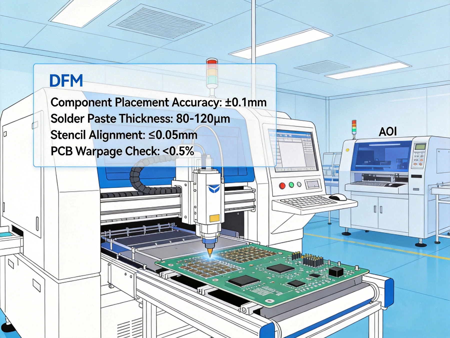
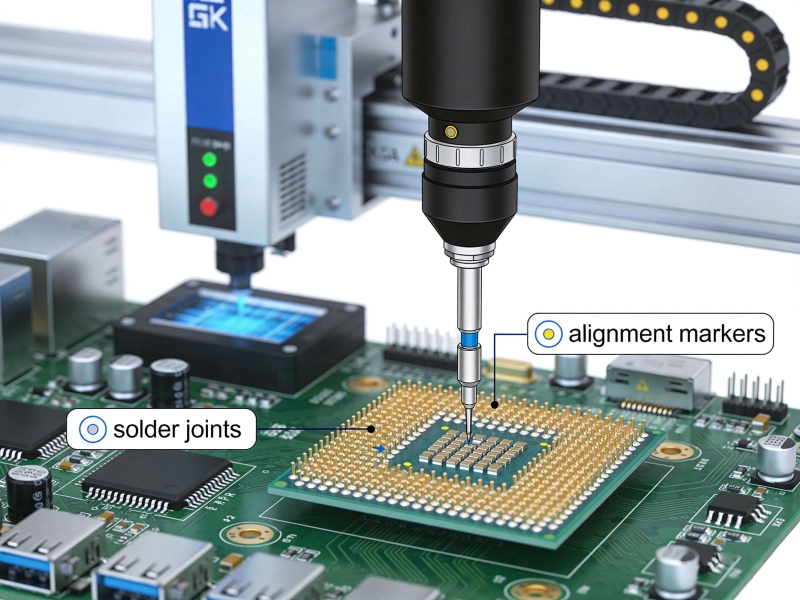
Global fiducial marks are mandatory for modern SMT equipment. Place three fiducials in a triangular pattern on the panel corners outside the assembly area. Each fiducial should be 1.0-1.5mm diameter with a 3mm clear area around it. Local fiducials for fine-pitch components (0.4mm pitch and below) should be placed within 5mm of the component footprint.
Chinese factories using Vision Inspection Systems rely heavily on fiducial recognition. Poor fiducial design accounts for approximately 8% of placement errors in our production data—entirely preventable with proper planning.
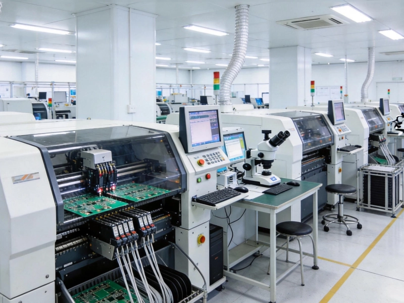
Modern pick-and-place equipment in Chinese factories operates at speeds exceeding 50,000 CPH for chip components. However, these machines have physical and optical constraints that designers must respect.
Maintain minimum spacing between components based on their height differential. For components of similar height (within 2mm), spacing of 0.5mm suffices. When tall components (over 3mm) neighbor short components, increase spacing to 1.5mm minimum to prevent collision during placement and allow for proper paste printing.
For BGA and QFN packages, provide a minimum 3mm clear zone around the component for rework access. This space also benefits Aoi Inspection visibility and post-solder cleaning access.
Standardize component orientation within each polarity group across the entire board. All polar capacitors, diodes, and ICs with pin 1 marking should face the same direction. This consistency dramatically improves placement accuracy and enables efficient batch processing.
We recommend orienting all components within 0°/90°/180°/270° angles only.斜角 placements (45°) complicate feeder configuration and reduce placement speed by up to 15% based on our equipment timing tests.
Leading Chinese SMT facilities now routinely handle 01005 components (0.4×0.2mm). However, these ultra-small parts require specific design considerations: pad size of 0.25×0.2mm with 0.1mm spacing, tight solder paste registration (≤50μm tolerance), and controlled humidity (RH below 60%).
If your design uses 01005 components, explicitly communicate this to your CM during DFM review. Not all factories have equal capability here—equipment age and operator expertise vary significantly.
Solder paste application is where most assembly defects originate. Statistics from our quality department show that 62% of first-pass yield issues trace back to paste printing problems—making stencil design a critical DFM consideration.
Stencil thickness selection depends on component pitch. For standard 0.5mm pitch components, use 0.12-0.15mm thick stencils with aperture reductions of 10-15% from pad size. For fine-pitch QFPs at 0.3mm pitch, consider 0.1mm thickness with 20% aperture reduction.
For QFN/SON packages with thermal pads, aperture design requires special attention. Use multiple small apertures (typically 0.8×0.8mm or cross-hatch patterns) rather than one large opening. This promotes consistent paste release and prevents voiding issues.
Lead-free solder (SAC305: Sn96.5Ag3.0Cu0.5) remains the standard for most China Manufacturing. Confirm your paste type matches your thermal profile. Type 3 or Type 4 powder is standard for most applications—Type 5 powder offers better paste release for ultra-fine pitch but requires compatible printing equipment.
For boards with thermal demands, consider high-temperature solders or specialized alloys. These require separate thermal profile development and should be flagged during DFM review.
Thermal Management during reflow affects everything from component survival to solder joint reliability. Chinese factories have diverse reflow oven capabilities, ranging from 8-zone to 14-zone systems.
For lead-free assemblies, standard profiles target peak temperatures of 245-250°C with time above liquidus (TAL) of 60-90 seconds. Ramp rates should stay between 1-3°C/second during preheat to prevent component stress. The cooling rate should not exceed 4°C/second to prevent tombstoning.
When designing thermal profiles, consider your board's thermal mass. Large ground planes, heavy copper weights (2oz+), and multilayer boards with internal planes require longer soak times and adjusted peak temperatures. Communicate these details during DFM—uneven heating causes warpage and delamination.
Identify temperature-sensitive components early. Certain LEDs, crystals, and polymer capacitors have maximum peak temperature limits below standard lead-free profiles. For these components, consider bottom-side placement, localized shielding, or pre-placement baking.
MSL (Moisture Sensitivity Level) components require special handling. All Level 2-5 parts must undergo baking before reflow if storage conditions were exceeded. Include MSL requirements in your DFM documentation to prevent popcorning failures.
Designing for testability reduces scrap, enables faster debugging, and supports long-term quality monitoring. Many designs look excellent functionally but prove impossible to test economically.
Include dedicated test points for all critical nets. We recommend a minimum of 4 test points per board—two for power rails and two for ground. For complex digital boards, consider allocating 10-15% of component count as test points.
Test pad diameter should be minimum 1.0mm for manual probing, 0.8mm for bed-of-nails fixtures. Via test points should be at least 1.2mm diameter with non-solder-mask-defined (NSMD) pads. Surface-mount test points allow faster in-circuit testing but require additional pad footprint space.
For boards with programmable devices, provide clear access to JTAG connectors. Standard 2×5 or 2×7 header positions should be documented with pinout specifications. Ensure mechanical clearance for programming cables—often overlooked in dense layouts.
Consider in-system programming (ISP) headers for firmware updates without IC removal. This becomes valuable during field support and reduces rework costs significantly.
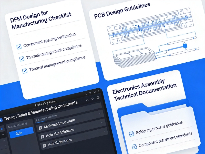
Complete documentation prevents misunderstandings and accelerates DFM review. Chinese factories expect specific information formats—learning these expectations improves collaboration.
Provide your CM with complete documentation packages: Gerber files (RS-274X format), NC drill files, pick-and-place files (centroid data), bill of materials (BOM), assembly drawings with layer definitions, and stack-up specifications for multilayers.
BOM formatting matters. Use standard templates with columns for: Item number, Reference designators, Quantity, Manufacturer part number, Manufacturer name, and any special handling notes. Two-supplier BOMs with alternate parts should clearly indicate primary vs. alternate status.
Document any special requirements explicitly: Conformal Coating, underfill, partial assembly, hardware installation, or custom test procedures. These requirements significantly impact production planning and should be communicated during initial DFM discussions, not discovered during production.
Include your quality expectations in writing—acceptable defect rates (typically PPM targets), inspection standards (Ipc-a-610 Class 2 or 3), and any industry-specific compliance requirements (ISO, IATF, UL).
Use this checklist during your design phase to catch common issues before they reach production:
Most Chinese PCB assembly factories complete DFM reviews within 2-5 business days. Complex multilayer or high-mix boards may take longer. We recommend building DFM review time into your project schedule—rushing this phase often leads to production issues.
DFM review fees vary widely—some factories include basic reviews in NRE costs, while complex military or aerospace DFM can run $500-2000+. Most commercial electronics DFM falls between $100-500. Consider this an investment: our data shows proper DFM reduces production scrap by 3-8%.
Both approaches have merit. Factory-provided DFM reflects their specific capabilities and limitations. Independent DFM services offer broader industry knowledge but may miss factory-specific constraints. For critical products, we recommend factory DFM as the primary review, supplemented by independent review for complex or high-reliability designs.
DFM benefits scale with volume. High-mix, low-volume production (under 100 units) may not justify extensive DFM investment—focus on critical checkpoints instead. For production runs exceeding 500 units, comprehensive DFM pays for itself quickly through improved yield and reduced rework.
Review your DFM guidelines annually at minimum. Manufacturing capabilities evolve rapidly—new equipment, materials, and process improvements change what's manufacturable. Chinese factories especially invest heavily in new capabilities, so annual DFM reviews often reveal new options for cost reduction or quality improvement.
Design For Manufacturability isn't a one-time checklist—it's an ongoing discipline that improves with experience and collaboration. By understanding manufacturing constraints early in design, engineers reduce costly respins, accelerate time-to-market, and build stronger relationships with their Chinese assembly partners.
The 2026 guidelines presented here reflect current capabilities across leading Chinese SMT facilities, but specifics vary by factory and equipment generation. Always confirm capabilities with your specific CM and engage them early in the design process.
Effective DFM collaboration starts with clear communication, complete documentation, and mutual respect between design and manufacturing teams. When both parties share knowledge freely, the result is better products, lower costs, and faster delivery schedules—benefits that compound across every production run.

How to Reduce SMT PCB Assembly Costs in China with Early DFM AnalysisJune/17/2026
Essential DFM Guidelines for SMT PCB Assembly in ChinaMay/29/2026

Optimizing PCB Design for Chinese SMT ManufacturersJuly/02/2026
Top 10 DFM Mistakes to Avoid Before Sending Files to China for SMT AssemblyJuly/14/2026
Overcoming BGA Challenges in a Complex SMT PCB Assembly China ProjectMay/29/2026
The Complete Process WalkthroughMay/29/2026
Overcoming BGA Challenges in a Complex SMT PCB Assembly China ProjectJune/09/2026
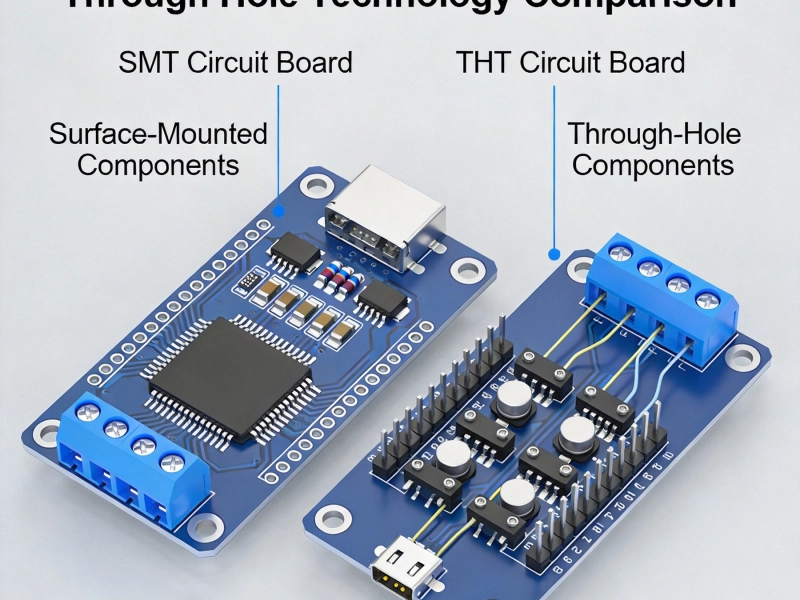
Which Technology is Right for Your Project?May/29/2026