Ever wondered what really goes on inside a top-tier Smt Pcb Assembly factory in China? Most people see finished products, but the journey from bare board to assembled board involves multiple precise steps, specialized equipment, and skilled operators. Top Chinese SMT factories combine advanced automation with quality processes that deliver millions of assembled PCBs daily.
In this walkthrough, we'll take you inside a leading Smt Assembly facility and show you exactly what happens at each stage. From initial PCB fabrication to final testing and packaging, you'll understand the complete process that turns your design files into physical circuit boards. Whether you're an engineer looking to understand the assembly side or someone considering manufacturing in China, this gives you the inside view.

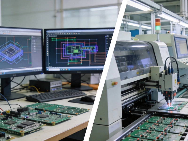
Before any component assembly can happen, you need a bare PCB. Most top SMT facilities either have in-house PCB fabrication or work with trusted partner fabs. The PCB fabrication process involves multiple steps from design data to finished boards.
PCB fabrication steps:
Top facilities implement statistical process control throughout fabrication. They track defect rates, identify problem areas, and continuously improve processes. This focus on quality at the source prevents problems from reaching assembly.
Once bare boards arrive at the assembly line, they undergo thorough inspection and preparation. This quality gate prevents defective boards from entering assembly and wasting components and machine time.
Pre-assembly inspection steps:
Boards that pass inspection move forward to component preparation. Boards that fail either get reworked or rejected, preventing defective boards from progressing through the expensive assembly process.
The quality of assembled boards depends significantly on component quality. Top SMT facilities have robust component management processes that ensure proper components are available and properly stored.
Component management:
Top facilities track component lots for traceability. If a component issue emerges, they can trace back to specific production lots and identify affected products. This traceability is crucial for quality management and customer communication.
Components need to be loaded onto feeders that feed the pick-and-place machines. This看似 simple step requires careful attention to ensure correct components in the correct orientations.
Feeder preparation process:
Mistakes at this stage - wrong component, wrong orientation, or damaged components - create defects later that are expensive to fix. Top facilities implement multiple verification steps and sometimes use vision systems to verify component identity.
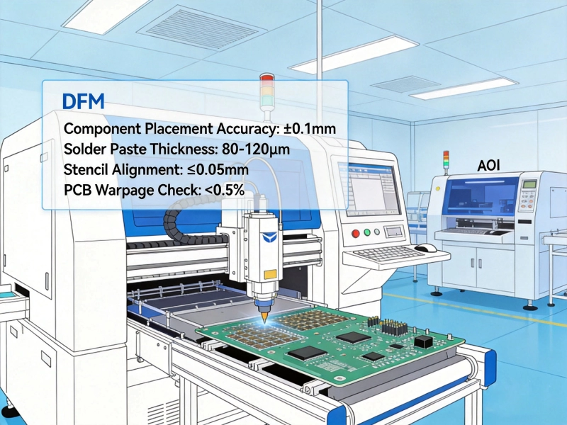
Solder Paste Printing is one of the most critical Smt Assembly steps. The paste must deposit precisely on component pads in the right amount. Poor paste application causes solder defects that are difficult to detect until later.
Solder Paste Printing process:
Solder paste quality factors:
Top facilities use automated solder paste inspection (SPI) systems that measure paste deposit volume and geometry. SPI catches problems early, allowing correction before components are placed. This prevents assembly failures that would be much more expensive to fix later.
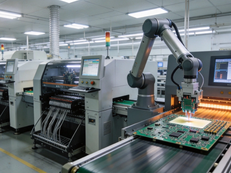
Modern pick and place machines are the heart of SMT assembly. These machines pick components from feeders and place them precisely on PCB pads. Top facilities operate multiple machines in assembly lines that can place thousands of components per hour.
Pick and place process:
Modern pick and place capabilities:
Top facilities maintain their pick and place equipment meticulously. Regular calibration, nozzle replacement, and preventive maintenance ensure consistent placement accuracy. Production data is tracked and analyzed to identify trends that indicate maintenance needs.
Component placement accuracy directly affects solder joint quality. Components placed off-position create defective solder joints. Modern machines achieve remarkable accuracy, but verification is still important.
Placement verification methods:
Top facilities set acceptance criteria for placement accuracy. Components outside tolerance get flagged for rework. This quality control prevents defective assemblies from progressing through the process.
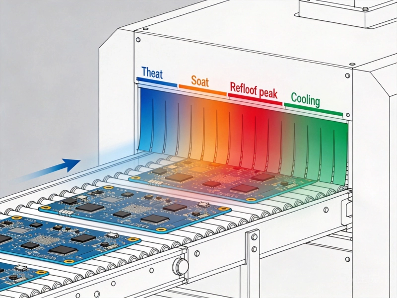
Reflow Soldering melts solder paste to create solder joints. The thermal profile - the temperature curve over time - must be optimized for your specific PCB, components, and solder paste. Wrong profiles cause solder defects like tombstoning, bridging, or cold solder joints.
Reflow Profile phases:
Profile development process:
Top facilities save optimized profiles for reuse on similar products. They also track profile performance data to identify when profiles need adjustment. This data-driven approach ensures consistent soldering quality.
Modern reflow ovens provide precise temperature control through multiple heating zones and forced convection. The right equipment and proper operation are essential for reliable soldering.
Reflow oven features:
Reflow process control:
Top facilities perform regular Reflow Profile verification. They measure actual temperature profiles on boards to confirm ovens are performing as expected. This proactive approach catches equipment problems before they cause quality issues.
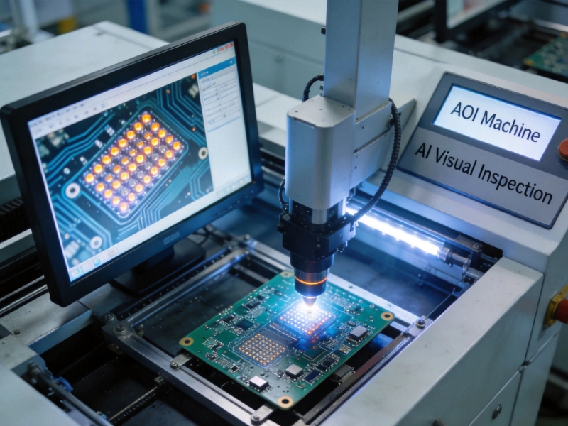
After reflow, boards undergo Automated Optical Inspection to catch defects before they progress further in the process. Aoi systems use cameras and image analysis to identify solder defects, component placement issues, and other problems.
Aoi Inspection targets:
Aoi technology:
AOI significantly improves quality by catching defects that would be difficult or impossible to detect with human inspection alone. Top facilities tune their AOI systems based on their specific products and defect profiles.
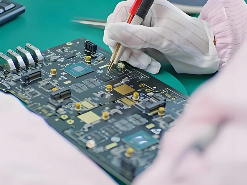
Boards flagged by AOI undergo rework to correct identified defects. Skilled technicians use specialized rework equipment to fix specific problems without damaging nearby components.
Common rework procedures:
Rework equipment:
Top facilities track rework data to identify systematic problems. If certain defects occur repeatedly, they investigate root causes and implement process improvements to prevent recurrence.
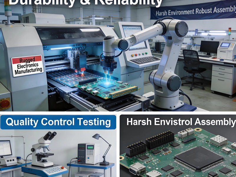
While SMT is dominant in modern electronics, many products still require some through-hole components. These larger components provide mechanical strength, better power handling, or connector interfaces that SMT components can't match.
Through-hole assembly processes:
Wave soldering process:
Top facilities carefully sequence SMT and through-hole operations. Typically, SMT assembly happens first, followed by through-hole assembly. This sequence prevents damage to SMT components during through-hole processing.
Wave soldering quality depends on proper equipment setup and process control. Poor wave soldering causes defects like solder bridges, insufficient solder, or cold solder joints.
Wave soldering optimization factors:
Top facilities use automated wave soldering machines with precise controls. They monitor solder pot chemistry regularly and replace solder as needed to maintain consistent soldering performance.
In-circuit testing verifies electrical connectivity and component values on assembled boards. ICT fixtures make electrical contact to test points, allowing the system to measure resistances, capacitances, and other electrical characteristics.
ICT capabilities:
ICT advantages:
Top facilities develop comprehensive ICT test programs that verify critical electrical characteristics. They maintain ICT fixtures carefully and replace worn probes to ensure reliable electrical contact.
While ICT checks component-level functionality, functional testing verifies that the assembled board performs its intended function. This might include powering the board and checking outputs, running test software, or simulating actual operating conditions.
Functional test approaches:
Functional testing often requires custom test fixtures and software. Top facilities work with customers to develop appropriate functional tests that verify board performance in ways that matter for end-use applications.
Before boards are packaged and shipped, they undergo final inspection. This catch-all inspection identifies any remaining issues that previous tests might have missed.
Final inspection checklist:
Boards that pass final inspection move to packaging. Boards that fail undergo appropriate rework or rejection based on the nature of the defect.
Static electricity can damage electronic components, so proper ESD protection is essential throughout assembly and especially during packaging and shipping.
ESD protection measures:
Top facilities have comprehensive ESD control programs. They regularly test ESD protection equipment and train personnel on proper ESD procedures.
Many electronic components and assembled boards are sensitive to moisture. Moisture absorbed during assembly or storage can cause problems during soldering or later operation.
Moisture sensitivity measures:
Top facilities follow IPC moisture sensitivity guidelines (MSL) for packaging and storage. They track moisture sensitivity levels for products and ensure appropriate handling throughout the process.
Complete documentation and traceability are essential for quality management and customer requirements. Top facilities maintain detailed records throughout the assembly process.
Documentation includes:
Top facilities use manufacturing execution systems (MES) that track each board through the process and maintain comprehensive records. This traceability allows quick response to any quality issues that emerge in the field.
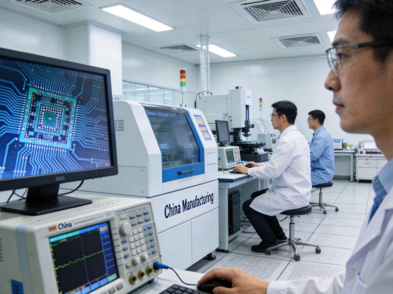
Top SMT assembly facilities operate under formal quality management systems. ISO 9001 certification is common, and many facilities have additional certifications specific to their industries or customer requirements.
Common certifications:
These certifications require documented processes, regular audits, and continuous improvement. Top facilities take quality systems seriously and invest in maintaining certifications and improving processes.
Quality isn't static - top facilities continuously improve processes based on data, feedback, and changing requirements. This commitment to improvement keeps them competitive and responsive to customer needs.
Continuous improvement activities:
Top facilities track quality metrics and set improvement goals. They use this data to drive decisions about equipment investments, process changes, and training needs.
If you're considering SMT assembly in China, choosing the right partner matters. Not all facilities have the same capabilities, quality systems, or commitment to service.
Key selection criteria:
Look for facilities that have experience with products similar to yours. A facility that assembles high-density consumer electronics might not be ideal for industrial control boards, and vice versa. Experience in your specific product type matters.
When evaluating potential partners, ask the right questions to understand their capabilities and approach:
Essential questions:
Pay attention to how they communicate. A partner who's responsive and communicative during evaluation will likely be responsive and communicative during production.
Top SMT assembly facilities in China combine advanced equipment, skilled personnel, and rigorous quality processes to deliver high-quality assembled PCBs efficiently. From PCB fabrication through component placement, soldering, inspection, testing, and packaging, each step involves specific technologies and procedures that ensure reliable results.
The key to success is attention to detail at every step. Poor quality at any stage - bare Pcb Defects, wrong components, improper soldering, or inadequate testing - affects final product quality. Top facilities understand this interdependence and implement quality controls throughout the process.
For anyone considering SMT assembly in China, understanding this complete process helps you make informed decisions about manufacturing partners and set appropriate expectations for production. The capabilities and quality systems we've described represent what you should expect from a top-tier facility.
Modern electronics depend on reliable SMT assembly. The processes, equipment, and quality systems we've explored make that reliability possible at the scale required for global electronics production.
Q: How long does Smt Pcb Assembly typically take?
A: Turnaround time varies based on order size and complexity. Simple prototypes might take 3-5 days. Production runs might take 1-3 weeks depending on volume. Rush services are available at premium cost. The facility's current workload also affects timing.
Q: What's the typical yield in a well-run SMT assembly line?
A>High-quality facilities typically achieve first-pass yields above 98% for most products. Complex designs with very small components might have slightly lower yields initially but improve as processes are optimized. Continuous improvement drives yields higher over time.
Q: Can I mix SMT and through-hole components on the same PCB?
A>Yes, mixed technology boards are common. The typical sequence is SMT assembly first, followed by through-hole assembly. The through-hole process (wave soldering) is designed to not damage previously placed SMT components. Selective soldering can be used for sensitive SMT components.
Q: How do I know which PCB surface finish is best for my application?
A>Surface finish choice depends on your application and requirements. HASL is cost-effective but less flat. ENIG provides flat surfaces and good shelf life. OSP is lead-free and cost-effective but has limited shelf life. Consider component types, storage time, and cost when choosing.
Q: What happens if my assembled boards have quality issues?
A>Top facilities have Quality Assurance processes to catch issues before shipment. If issues emerge in the field, facilities will investigate root cause, implement corrective actions, and potentially rework or replace affected products depending on the nature and extent of the issue. The response depends on warranty terms and the specific situation.
The Role of Automated Optical Inspection (AOI) in China's SMT Assembly LinesJune/16/2026
Step-by-Step: From Solder Paste Printing to Final Testing in China SMT AssemblyJuly/13/2026
Understanding Reflow Soldering Profiles Used in SMT PCB Assembly ChinaJune/30/2026
How a Top High Frequency PCB Manufacturer Ensures Signal IntegrityJune/02/2026
Essential DFM Guidelines for SMT PCB Assembly in ChinaJune/04/2026
Overcoming BGA Challenges in a Complex SMT PCB Assembly China ProjectMay/29/2026
How We Helped a US Startup Scale from Prototype to Mass SMT Assembly in ChinaJuly/07/2026
The Demands of Industrial SMT PCB Assembly in ChinaMay/29/2026