China has been the world's dominant center of Electronics Manufacturing for over two decades, and for good reason: the combination of deep supply chains, experienced workforce, equipment density, and cost efficiency is difficult to replicate anywhere else. For companies that design in California or Munich and manufacture in Shenzhen, Dongguan, or Suzhou, the PCB stack-up is one of the most consequential design decisions—and one of the most likely to cause problems if it is not made with the realities of Chinese supply chains firmly in mind.
Working with a Chinese Contract Manufacturer (CM) for Smt Assembly is not fundamentally different from working with one in Europe or North America in principle. The same physics applies, the same Ipc Standards govern quality, and the same stack-up rules hold. But Chinese CMs often serve hundreds of customers simultaneously, source materials from a wider range of suppliers, and may have different default assumptions about acceptable process windows. A stack-up that is perfectly adequate for a dedicated, High-mix Low-volume facility may cause repeated failures at a high-volume Chinese assembly line unless it is designed with that specific environment in mind.
This article focuses on the stack-up considerations that matter most for reliable Smt Assembly in Chinese supply chains: material selection, Thermal Management, Warpage Control, copper balance, solder mask, and the Dfm process that connects stack-up design to assembly execution.

The Chinese SMT Landscape: What Affects Stack-up Decisions
Before diving into stack-up specifics, it helps to understand the structural features of Chinese SMT assembly that influence design decisions:
Volume vs. Flexibility Trade-off
Many Chinese CMs are optimized for high throughput—lines running at 80,000+ components per hour with minimal changeover time. This efficiency comes with less flexibility to accommodate unusual stack-ups, exotic materials, or non-standard processes. A stack-up that requires a non-standard Reflow Profile, a specialty laminate, or a unique solder mask will likely encounter longer lead times, higher unit cost, or reduced yield at a high-volume CM compared to a dedicated prototype or low-volume facility.
The practical implication: design your stack-up to use materials and processes that are in the CM's standard repertoire. Specialty materials are fine if you are working with a CM that specializes in your product category—but risky if you are a small customer on a general-purpose line.
Material Sourcing and Traceability
Chinese CMs typically source laminate from domestic suppliers (Kingboard, Shengyi, Huaxin) alongside international brands (Nan Ya, Isola, Rogers). The laminate market in China is competitive and varied, with quality ranging from world-class to substandard. Your stack-up specification should include explicit material callouts—not just "FR-4" but "Shengyi S1000-2, Tg 150 °C, Dk 4.2 at 1 GHz." Without a specific callout, the CM's default material may be adequate—or it may not.
For products requiring Controlled Impedance or high reliability, require material certificates (Dk/Df test reports, lot Traceability) with each production lot. A good Chinese CM will provide these; a poor one will not, and the absence of Traceability is a warning sign.
Labor and Process Consistency
Chinese assembly lines employ skilled operators, but turnover rates in the Electronics Manufacturing sector are high. Process consistency depends heavily on written procedures, well-trained operators, and robust equipment calibration—not on individual craftsmanship. Your stack-up and Dfm documentation must be precise enough that a less experienced operator can produce the same result as a senior one. This means clear specifications, explicit tolerances, and unambiguous process instructions—not vague design rules.
Thermal Management: Tg Selection and Thermal Cycling
The glass transition temperature (Tg) of the PCB laminate is the single most important thermal parameter for SMT assembly. Tg is the temperature at which the epoxy matrix transitions from a rigid glass to a rubbery state—losing stiffness and potentially deforming. Every Smt Assembly Process subjects the board to multiple thermal cycles: solder paste reflow (peak 230–260 °C for lead-free), selective wave or repair rework (potentially higher), and in-field thermal cycling during use.
Tg Categories and Their Assembly Implications
-
Standard FR-4 (Tg 130–140 °C): The most common and least expensive laminate. Adequate for single-pass lead-free reflow if the peak temperature stays below ~245 °C and the time above liquidus (TAL) is under 60 seconds. Not recommended for boards that will see rework or high-temperature in-field operation.
-
Mid-Tg FR-4 (Tg 150–170 °C): The workhorse of Chinese SMT assembly. Provides a 20–30 °C margin above the lead-free reflow peak, reducing the risk of delamination or warpage during the assembly process. Suitable for most commercial and industrial products.
-
High-Tg FR-4 (Tg 170–180 °C): Required for boards with multiple reflow passes (e.g., boards with bottom-side BGAs that are reflowed twice), Lead-free Assembly of large boards with high thermal mass, or applications with high in-field operating temperatures. Also preferred for boards with heavy copper (3 oz or 4 oz outer layers), which requires higher press temperatures and longer lamination cycles.
-
High-Tg and high-CTE laminates (Tg > 180 °C): Used for automotive under-hood applications, LED lighting with high drive currents, and any product with an operating temperature above 125 °C.
Why Tg Matters More in Chinese Assembly
Chinese SMT lines are often optimized for throughput, which can mean faster conveyor speeds and shorter preheat ramp rates. On large, thermally massive boards, fast ramp rates create temperature gradients across the board—the center heats faster than the edges, creating mechanical stress. A laminate with adequate Tg margin will absorb this stress without deformation; a laminate at the edge of its thermal capability may warp, delaminate, or develop barrel cracks in plated through-holes. Specifying mid-Tg or high-Tg laminate for production runs in China is cheap insurance against these failures.
Warpage Control: The Enemy of High-Yield SMT
Board warpage is the leading cause of assembly defects in high-volume SMT lines: tombstoning, bridging, non-wetting opens, and misaligned placements all correlate with board warpage. In a Chinese CM's high-throughput environment, even a small percentage of warped boards creates significant yield loss across thousands of assemblies.
What Causes Warpage
-
Asymmetric copper distribution. If the copper coverage differs significantly between the top and bottom layers, or between different layers on the same side, the board will warp during lamination (because each layer cures with different residual stress) and during reflow (because each layer expands differently with temperature).
-
Thermal mass variation. Large copper areas (ground planes, large pads) adjacent to thin-trace areas create thermal gradients during reflow. The board bends toward the area that heats faster.
-
Residual lamination stress. Improper press cycle (wrong pressure, temperature ramp rate, or cooling rate) leaves residual stress in the laminate that manifests as warpage after routing or depanelization.
-
Board thickness. Thin boards (< 1.0 mm) warp more easily than thick boards. This is especially relevant for portable and wearable products where the CM may need to use thinner boards than the design originally specified.
Stack-up Rules to Prevent Warpage
-
Balance copper across the board centerline. For a symmetric stack-up, the copper coverage on Layer 1 should approximately match Layer N, Layer 2 should match Layer N−1, and so on. A 10 % copper imbalance is tolerable; a 50 % imbalance is not.
-
Use a symmetric stack-up. Mirror the layer structure around the board centerline. A 6-layer stack-up of Signal–Ground–Power–Power–Ground–Signal is symmetric and warp-resistant. Signal–Ground–Signal–Signal–Ground–Signal is asymmetric and prone to warpage.
-
Specify copper weight balance between outer layers. If the top layer has 40 % copper fill, the bottom layer should also have approximately 40 %. This is especially important for boards with large copper pours on one side and sparse routing on the other.
-
Specify minimum board thickness for your application. If your product fits within a 1.6 mm board, do not default to 0.8 mm to save cost—the thinner board will warp more and increase assembly defects. The cost saving in laminate will be dwarfed by the cost of reworking warped assemblies.
Copper Balance and Layer Distribution
Copper balance is closely related to Warpage Control but deserves its own treatment because it has additional implications for Smt Assembly Quality beyond mechanical flatness.
Ground and Power Plane Distribution
-
Distribute ground and power planes symmetrically. In a 6-layer board, placing both ground planes adjacent to the center (G1–G2) and both power planes adjacent to the outer signal layers creates an asymmetric field that concentrates stress. Instead, alternate ground and power layers: Signal–Ground–Power–Ground–Power–Signal, or distribute them symmetrically around the center.
-
Fill unused board area with copper. Empty areas on inner signal layers are a copper imbalance risk. Adding copper fills (connected to the nearest reference plane) to unused areas balances copper and improves EMI shielding—without changing the electrical design.
Heavy Copper and Thermal Relief
For boards that include power distribution sections with heavy copper (2 oz or 3 oz), the transition between heavy-copper zones and standard-copper zones must be managed carefully:
-
Stepped lamination (using different copper weights on different areas of the same layer) is possible but expensive and rarely used. Instead, use uniform copper weight across the panel and route heavy traces as wide traces on standard-copper layers.
-
Thermal relief connections between large component pads and the copper plane prevent heat sinking during soldering—which would prevent the pad from reaching reflow temperature. For BGAs and QFNs, full thermal connections (solid copper) are preferred for thermal performance; for SMD passive components, 4-strap thermal reliefs are standard.
Material Selection for SMT Assembly: Practical Guidance
FR-4 Grades in Common Chinese Use
-
Shengyi S1000-2 (Tg 150 °C): The most common mid-Tg laminate in Chinese fabs. Good process compatibility, widely available, competitive pricing. Suitable for most commercial SMT assembly.
-
Kingboard KB-6160 (Tg 150 °C): Equivalent to S1000-2, widely stocked. Another reliable mid-Tg option.
-
Nanya NP-140L (Tg 140 °C): A good standard-Tg laminate from a Taiwanese supplier with strong presence in China. Use where Tg 140 is acceptable for the assembly profile.
-
Isola DE-104 (Tg 180 °C): High-Tg, lead-free compatible, excellent CAF resistance. Use for demanding applications, multiple reflow passes, or high-power boards.
Lead-Free Compatibility
All laminates used for Lead-free Assembly (which is now effectively universal in Chinese manufacturing) should be specified as lead-free compatible or long-term thermal resistance rated. This designation means the laminate has passed 288 °C immersion testing and does not delaminate at the lead-free reflow peak temperature of 260 °C. Standard, non-lead-free-rated FR-4 can delaminate during lead-free reflow even if the Tg is nominally adequate.
Dk and Df for Mixed-Signal Boards
If your board includes high-speed digital signals (PCIe, USB 3.0, 1 Gbps Ethernet) alongside SMT components, you need to consider Signal Integrity as well as SMT assembly reliability. The key parameters are:
-
Dk (dielectric constant) affects trace impedance. For controlled-impedance traces, specify the Dk and verify that the CM uses a material lot with Dk within ±0.05 of your target. Standard FR-4 has Dk 4.2–4.5 at 1 GHz with ±0.2 lot-to-lot variation—wide enough to affect ±7 % impedance tolerance.
-
Df (dissipation factor) affects signal loss at high frequencies. For 1 Gbps and above, specify low-loss or mid-loss laminate (Df ≤ 0.015). Standard FR-4 (Df ≈ 0.02) is adequate for 100 Mbps and below.
Solder Mask: The Overlooked Stack-up Element
Solder mask is a polymer coating that defines which copper areas are solderable and which are not. Its properties directly affect SMT assembly yield and reliability:
Solder Mask Thickness and Variability
-
Nominal thickness: 0.8–1.2 mil (20–30 µm) over copper. Thinner mask provides better resolution for fine-pitch components; thicker mask provides better dielectric insulation and moisture barrier.
-
Thickness variability: The thickness variation across a panel (typically ±20 % of nominal) is the main source of problems. At via-in-pad (VIP) structures, thin solder mask can wick into the via during coating, leaving a void that exposes copper. At fine-pitch components, thick mask in the pad area can reduce solder joint coplanarity.
-
Specification: Specify the solder mask type (PSR-4000, DPS, or equivalent), color (green is most common and most process-proven; other colors may have different thickness characteristics), and any specific openings (VIP openings, RF area clearances).
Solder Mask Color and Assembly Considerations
-
Green solder mask is the standard for a reason: it is the most process-mature, the most compatible with Aoi Inspection (contrast with copper is excellent), and the most stocked by CMs. Use green unless there is a compelling reason not to.
-
White mask reflects heat differently during reflow (slightly lower peak temperature on the board surface). For large, thermally heavy boards, this can cause cold joints on bottom-side components. Test before committing to white mask on multi-pass assemblies.
-
Black mask absorbs more heat, raising board surface temperature during reflow. It also makes Aoi more difficult (poor contrast with copper) and increases the risk of missed defects. Avoid for complex SMT boards unless aesthetics are paramount.
Stack-up Design for Specific SMT Challenges
Bottom-Side BGA Assembly
Boards with BGAs on both sides require particular stack-up attention. The bottom-side BGA is reflowed second, which means it sees two reflow cycles. The concerns are:
-
Lamination stress: Two-pass reflow exposes the board to thermal stress twice. A poorly laminated board may delaminate on the second pass. Specify high-Tg laminate (≥ 150 °C) and symmetric copper balance to minimize this risk.
-
Warpage: After the first reflow (top-side assembly), the board may have warped slightly. Bottom-side BGA placement and reflow on a warped board causes misalignment. A symmetric stack-up and adequate board thickness (≥ 1.2 mm for boards larger than 150 mm) reduce this risk.
-
Underfill compatibility: If your design uses capillary underfill for BGAs, the PCB surface must be clean and compatible with the underfill material. Confirm with the CM that the solder mask surface finish is appropriate for underfill adhesion.
Large Boards with High Thermal Mass
Large boards (> 250 mm in either dimension) with heavy components (large BGAs, QFPs, inductors) present assembly challenges because of thermal gradients during reflow:
-
Specify forced-air preheating in the Reflow Profile to reduce the temperature gradient across the board before the reflow zone.
-
Use thermocouple-based profiling on a representative board (with thermal mass equivalent to the production boards) to set the correct profile. Do not assume that a profile optimized for a small board works for a large one.
-
Specify 氮气回流 (nitrogen reflow) for large boards with critical BGAs—oxygen in the reflow atmosphere promotes oxidation and reduces wetting, especially on large solder joints where the time above liquidus is longer.
01005 and Fine-Pitch Components
For boards populated with 01005 passives (0.4 × 0.2 mm) and 0.4 mm pitch BGAs, the stack-up requirements become more stringent:
-
Board flatness: Warpage tolerance is tighter for fine-pitch assembly. Specify a warpage limit of ≤ 0.5 % (per IPC-A-600 Class 3) for boards with 0.4 mm pitch BGAs.
-
Solder paste volume control: The CM must use SPI (solder paste inspection) to verify paste volume on every pad for 01005 Components. A 10 % paste volume error on a 01005 land (tiny pad area) can cause a tombstone or bridge defect.
-
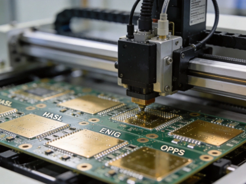
Plating thickness control: The ENIG plating thickness (Ni 3–5 µm, Au 0.05–0.10 µm) must be tightly controlled. Excessive gold thickness (> 0.15 µm) creates a brittle nickel-gold intermetallic that cracks under thermal cycling.
DFM Review: The Critical Connection Between Stack-up and Assembly
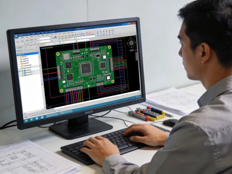
Design For Manufacturability review is the process where the stack-up meets the assembly process. In Chinese supply chains, DFM is especially important because the CM's engineering team may be working with your design for the first time, without the context that comes from an ongoing relationship.
Key DFM Items to Cover
-
Annular ring and drill size compatibility. Verify that all hole sizes are producible with adequate annular ring at the specified pad sizes. In Chinese fabs, minimum drill size is typically 0.2 mm for standard production; smaller drills may be available but add cost and reduce yield.
-
Pad size for via-in-pad. If you are using via-in-pad (VIP) for BGA breakout, verify that the CM can fill and planarize the via reliably. VIP under 0.5 mm pitch BGAs requires filled-and-capped microvias—not just tented vias.
-
Via capture pad size. For blind and buried vias, verify that the capture pad on the target layer is large enough for the laser drill registration tolerance (±0.05 mm typical).
-
Component keep-out zones. Specify keep-out zones for components that require hand repair or programming (connectors, memory sockets). If these zones overlap with high-density routing, the CM may route traces through them—creating an assembly conflict.
-
Test point accessibility. For ICT or flying-probe test, ensure that test points are accessible with probe tips (minimum 0.5 mm diameter probe pad, 3 mm spacing between adjacent pads). If test points are buried under tall components or in dense BGA escape routing, test coverage will be incomplete.
DFM Communication with Chinese CMs
Clear communication is the foundation of successful DFM with Chinese CMs. Best practices:
-
Provide a DFM checklist with your design files, listing the specific DFM items you want reviewed. Do not assume the CM will cover everything on their standard checklist.
-
Request DFM in writing and require a written response before manufacturing begins. Verbal DFM approvals are not traceable.
-
Use English or bilingual documentation for critical stack-up parameters. Even if the CM's engineers are fluent in English, technical terminology (Tg, Dk, Df, IPC class) should be explicit, not assumed.
-
Establish a clear escalation path. If the CM's DFM engineer raises a concern that conflicts with your design intent, you need a direct line to their engineering management—not just the sales contact.
Quality Standards and Inspection Criteria
When specifying quality requirements for SMT assembly in Chinese supply chains, be explicit about the standards and inspection criteria:
-
Ipc-a-610 Class 3 (Acceptability of Electronic Assemblies) is the standard for high-performance electronic products. Specify this class explicitly if your product is industrial, medical, automotive, or aerospace. Class 2 (commercial products) is less stringent and less costly; Class 1 (Consumer Electronics) is even more lenient. Using the wrong class creates quality disputes.
-
Solder joint acceptance criteria should reference specific Ipc-a-610 sections for the component types in your design. For BGAs, this includes minimum ball height, collapse height, and void criteria. For QFNs, it includes heel Fillet, side fillet, and thermal pad wetting requirements.
-
Aoi and X-ray requirements should be specified: 100 % AOI on all reflowed boards, 100 % X-ray Inspection on all BGA and QFN joints, and AQL (Acceptable Quality Level) for other defect types.
-
First-article inspection (FAI) should be required on the first production lot of a new product or after a significant design change. FAI includes full visual inspection, cross-section of representative solder joints, and X-ray of BGA joints.
Working with Chinese CMs: Practical Tips
-
Visit in person if possible—or send a qualified engineer. A CM relationship that is entirely remote is harder to manage than one with periodic face-to-face contact. A factory audit reveals capabilities (equipment age, cleanliness, process control) that are invisible over email.
-
Start with a pilot run before committing to high volume. A 50–100 unit pilot run reveals assembly process issues, material quality issues, and communication gaps that would be costly to discover in a 10,000-unit production run.
-
Document everything in writing. Verbal agreements about stack-up changes, material substitutions, or quality criteria are not legally binding in Chinese business practice and are frequently forgotten. Every decision should be documented in an email or formal change-control record.
-
Establish clear quality metrics at the start of the relationship: defect rate targets, defect type categories, reaction time for quality issues, and escalation procedures. Without agreed metrics, disputes about quality levels become circular.
-
Build a relationship with the CM's engineering team, not just the sales team. Engineers solve problems; sales people manage expectations. The best outcomes come from direct engineering-to-engineering communication about stack-up, process, and quality issues.
Conclusion
PCB stack-up design for SMT assembly in Chinese supply chains requires the same rigor as any other manufacturing environment—but with additional attention to the specific characteristics of Chinese manufacturing: high-volume throughput, broad material sourcing, process standardization, and the importance of written documentation at every step. The stack-up is not just an electrical design artifact; it is a manufacturing specification that determines assembly yield, quality, and cost.
The most common stack-up failures in Chinese SMT assembly are preventable: wrong Tg selection leading to delamination on lead-free reflow, copper imbalance causing warpage, vague material callouts enabling substitution with incompatible laminate, and missing Dfm Review allowing assembly-process conflicts to reach production. Each of these failures has a known solution that costs far less than the rework, delay, and relationship damage it prevents.
Spending an extra hour on the stack-up document, specifying materials by name and grade, balancing copper explicitly, and conducting a thorough Dfm Review with the CM before production are investments that pay back in yield, quality, and schedule confidence. In high-volume manufacturing, every tenth of a percent of yield improvement is worth thousands of dollars—and it starts with the stack-up.
For SMT PCB Assembly in China with full DFM review, IPC-A-610 Class 3 quality standards, and complete traceability, contact our engineering team to discuss your stack-up and assembly requirements.
FAQ
What Tg laminate should I specify for lead-free SMT assembly in China?
A Tg of 150 °C or higher is recommended for lead-free assembly. Standard FR-4 (Tg 130–140 °C) may be adequate for simple, single-pass assemblies, but mid-Tg (150 °C) or high-Tg (170+ °C) laminate provides better margin against delamination during the lead-free reflow peak of 250–260 °C.
How do I prevent board warpage during SMT assembly?
Use a symmetric stack-up with balanced copper coverage between opposite layers. Specify mid-Tg or high-Tg laminate for boards with multiple reflow passes or large thermal mass. Ensure outer-layer copper fill is balanced between top and bottom, and specify adequate board thickness for your product size.
Should I specify a specific laminate brand for my Chinese CM?
Yes. Specify by brand, grade, and Tg—not just "FR-4." Common options in Chinese supply chains include Shengyi S1000-2, Kingboard KB-6160 (both Tg 150 °C), and Nanya NP-140L. Specifying by name prevents the CM from substituting a lower-quality or incompatible material.
What quality standard should I specify for SMT assembly?
Specify IPC-A-610 Class 3 for industrial, medical, automotive, and aerospace products. Class 2 is acceptable for commercial products. Class 1 is for Consumer Electronics. Using the wrong class creates disputes about what constitutes an acceptable defect.
Why is DFM review especially important with Chinese CMs?
Chinese CMs serve many customers simultaneously and may be working with your design for the first time. Without a thorough DFM review, the CM may not catch design issues (pad sizes, keep-out zones, test point accessibility) that cause assembly defects or delays. A written DFM review with documented resolutions before production is the best protection.