China has become the world's Electronics Manufacturing powerhouse, but getting high-quality Smt Assembly from Chinese facilities requires more than just sending design files. The difference between designs that assemble smoothly and designs that create problems comes down to following best practices that respect both design requirements and manufacturing realities. We've worked with dozens of Chinese assembly facilities over the years, and this guide distills what we've learned into actionable best practices for high-quality Smt Assembly.
This ain't about design rules alone - it's about the practical strategies experienced designers use to ensure their designs assemble reliably, efficiently, and cost-effectively. Whether you're designing for high-volume production or low-volume prototyping, these best practices help you avoid common pitfalls and achieve consistent quality from your Chinese assembly partners.
Before diving into specific design practices, understand the Chinese Smt Manufacturing context. Chinese facilities operate at scale with sophisticated equipment, but they've optimized their processes for efficiency. Your design should work with their capabilities rather than against them.
Chinese assembly characteristics:
Top Chinese facilities can handle complex designs, but they prefer designs that align with standard processes. When you design within their standard capabilities, you get better results, lower costs, and faster turnaround.
Not all Chinese assembly facilities are equal. Selecting the right partner for your specific product type matters as much as following design best practices.
Partner selection considerations:
A facility experienced with consumer electronics might struggle with high-reliability industrial products. A facility focused on high volume might not be ideal for low-mix, low-volume production. Match your product type to their experience.
Your board's layer stack-up affects both electrical performance and manufacturability. Optimizing stack-up during design prevents problems that emerge later in production.
Stack-up optimization principles:
Common stack-up mistakes:
Work with your PCB fabricator on stack-up design early in the project. They can recommend standard stack-ups optimized for both fabrication and assembly. Standard stack-ups cost less and process more reliably than custom configurations.
Board dimensions affect manufacturability and assembly efficiency. Optimizing board size and shape during design saves money and improves production.
Board size considerations:
Board edge considerations:
For high-volume production, optimizing panel layout can reduce material costs significantly. Work with your assembly partner early to understand their panelization preferences.
Component selection affects manufacturability, cost, and availability. Smart component choices prevent assembly headaches.
Component selection principles:
Component size guidelines:
For low-volume or prototype runs, consider using slightly larger components to reduce assembly complexity. The size difference might not matter for your application, but the manufacturability improvement is significant.
How you place components affects assembly quality and efficiency. Good placement strategies prevent common assembly problems.
Placement strategy principles:
Spacing guidelines:
Consistent component orientation improves assembly efficiency and inspection reliability. Pick-and-place machines work faster when components have consistent orientation, and visual inspection becomes easier when orientation is predictable.
Trace width and spacing balance electrical requirements with fabrication capability. Proper trace design prevents fabrication and assembly problems.
Trace width guidelines:
Trace spacing guidelines:
For very dense routing, consider adding layers rather than pushing spacing limits. Adding a layer costs more but might be cheaper than fighting tight spacing constraints during assembly.
Reliable power distribution is essential for board performance. Good power distribution design prevents voltage drop, noise, and reliability problems.
Power distribution best practices:
Decoupling capacitor placement:
Decoupling capacitor placement affects power integrity more than many designers realize. The inductance between capacitor and IC determines effectiveness at high frequencies. Keep these connections short and direct.
Solder mask and pad design directly affect soldering quality. Good design prevents soldering defects like bridging and tombstoning.
Solder mask guidelines:
Pad design guidelines:
Use standard footprints from your EDA tool library when possible. Custom footprints should follow established guidelines. Avoid creating footprints from scratch without considering assembly requirements.
Thermal Management during assembly affects soldering quality and component reliability. Design Thermal Management properly from the start.
Thermal management considerations:
Temperature-sensitive components:
Thermal management during reflow is critical for reliability. Components that exceed their maximum temperature during soldering may fail immediately or develop reliability problems later.
Testable designs catch problems early and reduce test development time. Design testability in from the beginning rather than adding it later.
Testability design principles:
Test point guidelines:
Test points add cost through increased board area and test fixture complexity. Balance testability needs against cost. For high-volume production, good testability typically pays for itself through reduced test time and improved quality.
Design for visual inspection and Automated Optical Inspection (Aoi) catches defects early and improves quality.
Inspection design principles:
AOI is increasingly common in Chinese facilities. Designing for AOI improves inspection effectiveness and reduces false defect calls. When components have consistent orientation, AOI systems work more reliably.
Complete, accurate documentation prevents misunderstandings and delays. Provide everything the assembly facility needs upfront.
Essential documentation:
Documentation quality:
Chinese assembly facilities work with many customers. Complete, accurate documentation distinguishes professional designs from amateur efforts and prevents problems.
Good communication with your assembly partner prevents misunderstandings and ensures your requirements are met.
Communication principles:
Common communication mistakes:
Language and cultural differences sometimes cause communication gaps. Being explicit and documenting everything helps prevent misunderstandings.
Design choices significantly affect manufacturing cost. Optimizing for cost during design saves money without compromising quality.
Cost optimization principles:
Layer count vs. routing density:
Adding layers increases cost but might save money overall if it prevents fabrication problems or improves yield. Calculate total cost including yield and rework when comparing options.
Your production volume should influence design decisions. What works for high volume might not make sense for low volume, and vice versa.
High volume considerations:
Low volume considerations:
Match design complexity to volume. Over-engineering low-volume designs wastes money. Under-engineering high-volume designs causes problems that cost more to fix later.
Engage with your assembly partner before production for design review. Their input catches Dfm issues before they cause problems.
Pre-production review topics:
A good assembly partner provides constructive feedback. Take their suggestions seriously - they know what works in their production environment. Ignoring their expertise often leads to problems later.
After initial production, perform thorough first article inspection to confirm production meets requirements before committing to full production.
First article inspection items:
First article inspection catches problems early. Address issues before full production. This proactive approach prevents producing large quantities of defective boards.
These design mistakes appear repeatedly and cause avoidable problems. Avoiding them saves time, money, and frustration.
Most common design mistakes:
Design practices to avoid:
Many design mistakes result from rushing or not considering manufacturing consequences. Taking time for proper design review prevents problems that are much harder to fix later.
Pcb Design continues evolving with new technologies. Staying current helps you leverage advances in manufacturing capabilities.
Current trends:
Adoption considerations:
Use advanced technologies when they provide clear benefits. Don't use them just because they're available. Balance benefits against cost and complexity.
Environmental and sustainability concerns increasingly affect Pcb Design and assembly.
Sustainability considerations:
Sustainability requirements vary by market and application. Understand requirements for your target market and design accordingly.
Before starting layout, ensure you've addressed fundamental design considerations.
Pre-layout items:
Before sending design to production, verify all requirements are addressed.
Pre-production items:
Using checklists helps ensure you don't overlook critical items. Checking off items systematically prevents mistakes from rushing or oversight.
High-quality SMT assembly in China requires more than just following design rules - it requires understanding manufacturing realities, partnering effectively with assembly facilities, and designing for manufacturability alongside functionality. The best practices we've covered provide a framework for designs that assemble reliably, efficiently, and cost-effectively.
The key insight is that manufacturability should inform design decisions from the beginning. When you design with assembly in mind rather than treating manufacturability as an afterthought, you naturally avoid many common problems. Your designs work within standard capabilities rather than fighting them, and production proceeds smoothly rather than encountering constant problems.
Chinese assembly facilities are world-class when designs work within their optimized processes. Designing with their capabilities in mind gives you the full benefit of their expertise and equipment. When you fight against standard processes, you create unnecessary costs and delays that are entirely avoidable.
These best practices aren't theoretical - they come from real experience with Chinese assembly facilities and the lessons learned from hundreds of designs. Apply them to your designs, and you'll see the difference in production quality, cost, and reliability. Manufacturing success starts with design decisions made long before the first board reaches the assembly line.
Q: How do I know if my design is optimized for Chinese assembly?
A>Use the checklists provided and engage with your assembly partner for design review. Their specific feedback based on their capabilities provides the definitive assessment. If they identify no major concerns and provide minimal suggestions, your design is well-optimized.
Q: Should I design for the lowest possible cost or highest possible quality?
A>Aim for the optimal balance. Design for adequate quality at competitive cost. Don't compromise critical quality requirements to save small amounts of money. But don't over-engineer features that don't provide real benefit. The goal is cost-effectiveness, not minimum cost or maximum quality.
Q: How do I handle Chinese assembly facilities suggesting design changes?
A>Listen carefully to their suggestions. They know their capabilities and what works in their environment. Evaluate their suggestions objectively - some will improve manufacturability without compromising performance. Ask for specific reasoning and assess whether changes make sense for your requirements.
Q: What's the relationship between design complexity and assembly quality?
A>Complexity increases assembly risk and typically increases cost. Each additional layer, tight spacing requirement, or special process adds potential failure points. Balance complexity against actual requirements. Sometimes simpler designs achieve adequate performance at lower cost and higher reliability.
Q: How do I ensure my documentation is complete for Chinese assembly?
A>Use the documentation checklist provided. Have someone unfamiliar with your design review the files - if they can't understand what's needed, the documentation is incomplete. Be explicit about requirements rather than assuming understanding. When in doubt, provide more detail rather than less.
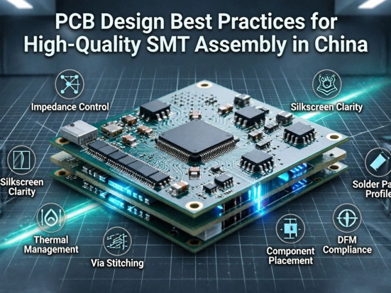
PCB Design Best Practices for High-Quality SMT Assembly in ChinaJune/05/2026
Thermal Management in PCB Design: Preventing Warpage in China's SMT AssemblyJuly/15/2026
How to Design the Perfect Land Pattern for SMT Components in Chinese FactoriesJune/18/2026
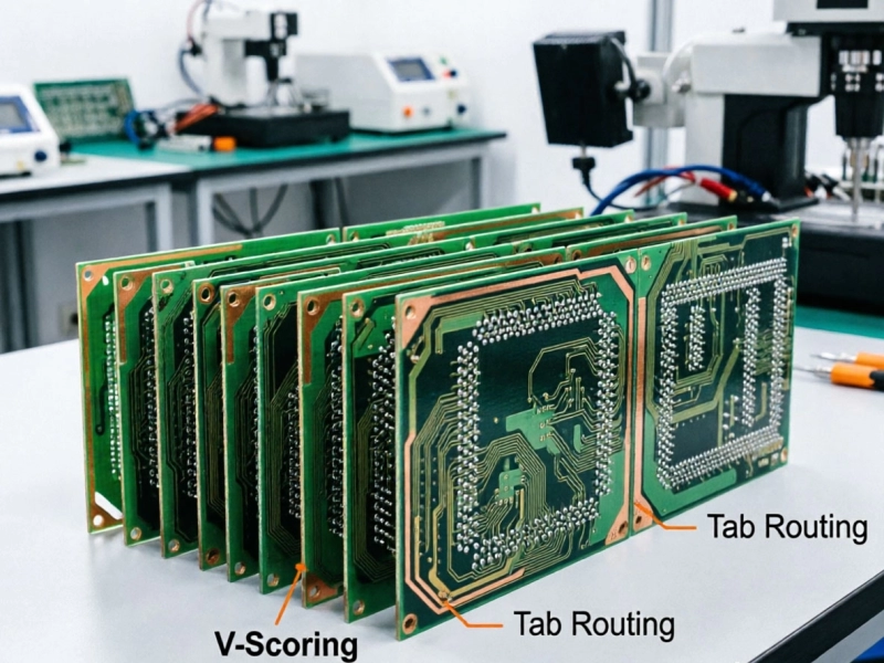
PCB Panelization Guide for SMT Assembly China: V-Scoring vs. Tab RoutingJuly/03/2026
Which Technology is Right for Your Project?May/29/2026
Overcoming BGA Challenges in a Complex SMT PCB Assembly China ProjectMay/29/2026
How We Helped a US Startup Scale from Prototype to Mass SMT Assembly in ChinaJuly/07/2026

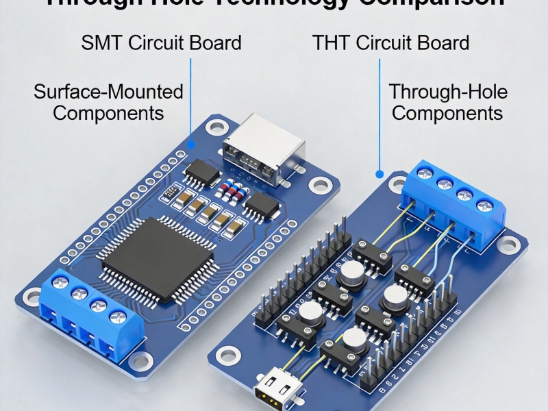
The Pros and Cons of SMT and THT in China's Electronics Manufacturing LandscapeJune/25/2026