Sending flawed design files to Chinese PCB manufacturers wastes weeks of time, thousands in rework costs, and damages critical supplier relationships.
China remains the world's leading destination for Pcb Assembly, offering competitive pricing, advanced capabilities, and massive production capacity. But sending design files across continents introduces risks that don't exist in domestic manufacturing. Communication barriers, time zone differences, and limited face-to-face interaction amplify the cost of design errors.
Design For Manufacturing (Dfm) problems discovered after files reach China trigger expensive cycles of clarification, redesign, and resubmission. What should be a straightforward production run becomes a drawn-out ordeal. This guide identifies the top 10 Dfm mistakes engineers make before sending files to China, and how to prevent them.

Why DFM Matters More with Chinese Manufacturing
Distance and communication barriers make DFM critical:
Communication Challenges
- Language barriers: Technical nuances lost in translation
- Time zone gaps: 12-15 hour delays for simple clarifications
- Cultural differences: Direct feedback sometimes softened or misinterpreted
- Documentation requirements: Complete, unambiguous specifications essential
Cost of Errors
- Shipping delays: Each correction cycle adds 2-4 weeks
- Rework costs: Engineering time to fix and resubmit designs
- Rush fees: Expedited shipping and production to recover schedule
- Reputation damage: Problematic files damage manufacturer relationships
Preventing DFM errors upfront eliminates these downstream costs.
Mistake #1: Incomplete or Inconsistent Gerber Files
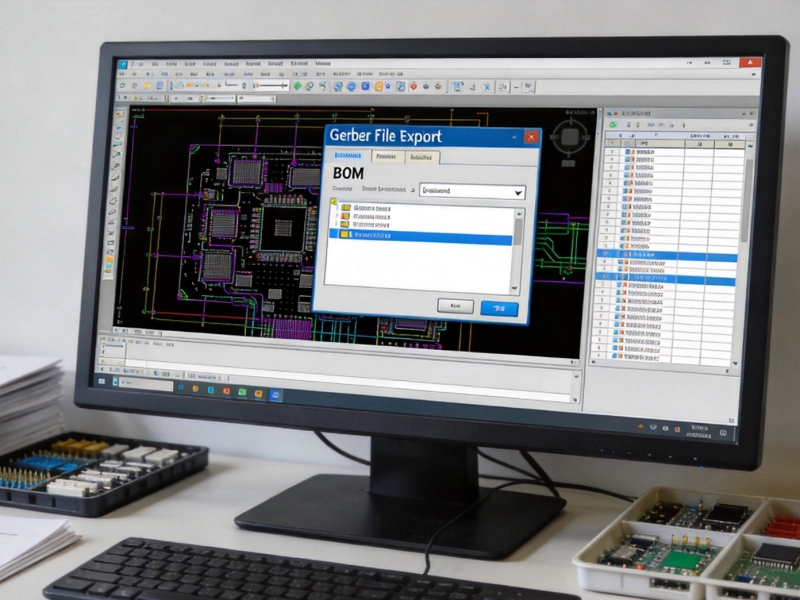
Gerber Files are the foundation of PCB Fabrication. Incomplete or inconsistent files cause immediate production delays.
Common Problems
- Missing layers: Not all copper layers included
- Format inconsistencies: Different formats for different layers
- Drill file mismatches: Drill coordinates don't match Gerber coordinates
- Missing apertures: Aperture definitions incomplete
- Incorrect file naming: Unclear layer identification
Solutions
- Use standard formats: RS-274X extended Gerber is universally accepted
- Verify completeness: Include all layers: copper, solder mask, silkscreen, drill, outline
- Check consistency: Ensure all files use same origin point and coordinate system
- Clear naming convention: Use descriptive file names (e.g., "Top_Copper.gtl", "Bottom_Copper.gbl")
- Include readme file: Document layer stack-up and special requirements
Mistake #2: Unclear or Missing BOM Information
The Bill of Materials (Bom) tells manufacturers what components to place. Ambiguity here creates assembly errors.
Common Problems
- Missing manufacturer part numbers: Only generic descriptions provided
- Outdated components: Parts specified are obsolete or unavailable
- Incorrect package types: Wrong footprints for specified components
- Missing reference designators: Component locations unclear
- No alternative parts: No substitutes when primary parts unavailable
Solutions
- Complete manufacturer part numbers: Include full MPN from authorized distributors
- Check availability: Verify parts are available before sending files
- Specify exact package: Include package type (e.g., "0603", "SOIC-8", "QFN-48")
- Clear reference designators: Ensure every component has unique, unambiguous designation
- Provide approved alternatives: List secondary part numbers for critical components
- Include distributor links: Provide direct links to component specifications
Mistake #3: Incorrect Component Footprints
Footprint errors cause components to fit poorly or not at all, leading to assembly defects.
Common Problems
- Land pattern mismatches: Pad sizes don't match component lead dimensions
- Wrong pad spacing: Pitch doesn't match component leads
- Missing thermal relief: Pads connected directly to planes without relief
- Courtyard violations: Components placed too close together
- Library part errors: Using unverified footprint libraries
Solutions
- Verify against datasheet: Check every footprint against manufacturer's land pattern recommendation
- Use Ipc Standards: Follow Ipc-7351 for Land Pattern Design
- Thermal relief for plane connections: Include proper thermal relief patterns
- Check courtyard spacing: Ensure minimum spacing between components
- Create custom footprints: Build verified footprints rather than relying on generic libraries
- 3D verification: Use 3D models to verify component fit
Mistake #4: Violating Minimum Spacing Requirements
Spacing violations create manufacturing defects and reduce assembly yield.
Common Problems
- Trace-to-trace spacing: Traces too close for reliable etching
- Pad-to-pad spacing: Component pads violate minimum spacing
- Via-to-feature spacing: Vias placed too close to other features
- Solder mask bridges: Insufficient mask between pads
- Copper-to-edge spacing: Traces too close to board edge
Solutions
- Know manufacturer's capabilities: Get minimum spacing specifications before designing
- Apply design rules: Use DRC (Design Rule Check) throughout design process
- Standard spacings: Use 6 mil trace/space minimum for standard production
- Solder mask dams: Ensure minimum 4 mil mask between adjacent pads
- Edge clearance: Maintain minimum 20 mil from copper to board edge
- Run DRC before sending: Verify all spacing rules pass before file release
Mistake #5: Ignoring Panelization Requirements
Panelization affects manufacturing efficiency and cost. Poor panelization wastes material and time.
Common Problems
- No panelization specified: Manufacturer must design panel, potentially inefficiently
- Poor board orientation: Boards oriented inefficiently on panel
- Missing fiducials: No global or local fiducial markers
- Insufficient margins: Boards too close to panel edges
- Wrong tooling hole locations: Tooling holes don't match assembly equipment
Solutions
- Consult manufacturer: Ask for preferred panel dimensions before designing
- Optimal panel size: Standard 16" x 18" or manufacturer's preferred size
- Include fiducials: Minimum 3 global fiducials plus local fiducials for fine-pitch components
- Adequate margins: Minimum 0.5" (12.7mm) margin around boards
- Tooling holes: Include 2-3 tooling holes per panel, minimum 3mm diameter
- Breakaway tabs: Specify mouse bites or V-score for board separation
Mistake #6: Failing to Specify Assembly Instructions
Assembly requires more than just Gerber Files and Bom. Missing instructions create errors.
Common Problems
- No assembly drawing: Component Placement unclear without visual reference
- Missing special instructions: Unusual requirements not communicated
- No test requirements: Testing procedures not specified
- Uncritical component marking: Critical components not identified
- No orientation indicators: Polarity and orientation unclear for polarized parts
Solutions
- Provide assembly drawing: Include visual Component Placement guide
- Mark polarity: Clear indicators for diodes, capacitors, ICs, connectors
- Specify special handling: ESD-sensitive components, moisture-sensitive devices
- Define test requirements: ICT points, functional test procedures, acceptance criteria
- Identify critical components: Mark components requiring specific manufacturers or grades
- Special assembly notes: Conformal Coating, washing requirements, special soldering profiles
Mistake #7: Overlooking Thermal Management Design
Thermal issues cause assembly defects and reliability failures.
Common Problems
- Thermal relief missing: Pads connected directly to large copper areas without relief
- Inadequate cooling for Power Components: No thermal vias or heat sinking
- Uneven thermal distribution: Hot spots created by poor component placement
- Missing thermal vias: Power devices without heat transfer paths
- Reflow Profile concerns: Design incompatible with standard reflow profiles
Solutions
- Thermal relief patterns: Connect pads to planes with proper thermal relief (minimum 4 spokes)
- Thermal vias under Power Components: Multiple vias under thermal pads
- Component spacing for heat: Adequate spacing around high-power components
- Copper pours for heat spreading: Use large copper areas to spread heat
- Consider reflow process: Ensure design works with standard 3-zone or 7-zone reflow
Mistake #8: Incomplete or Missing Test Points
Testing reveals manufacturing defects and verifies functionality. Missing test points make testing difficult or impossible.
Common Problems
- No test points specified: Critical signals inaccessible for testing
- Test point spacing violations: Points too close for probe cards
- Wrong test point locations: Points placed in inaccessible locations
- Missing ground references: No ground points for probe grounding
- Test points under components: Points covered by components
Solutions
- Add test points for all critical signals: Power, ground, clocks, resets, critical data lines
- Standard test point spacing: Minimum 50-100 mil between test points
- Accessible locations: Place test points away from components, near board edges
- Ground points: Include multiple ground test points distributed across board
- Test point size: Minimum 40 mil diameter for reliable probing
- Test point documentation: Provide test point coordinate file and schematic reference
Mistake #9: Neglecting Silkscreen and Documentation Quality
Silkscreen and documentation aid assembly, testing, and debugging. Poor quality creates confusion.
Common Problems
- Missing reference designators: Component locations not marked
- Small or illegible text: Text size below readable limits
- Text over pads or vias: Silkscreen overlaps solderable features
- Missing polarity indicators: Orientation not marked
- Missing critical labels: Board name, revision, date not marked
Solutions
- Include all reference designators: Mark every component location
- Minimum text size: Use minimum 40 mil height, 6 mil line width
- Avoid overlap: Keep silkscreen away from pads and vias
- Polarity marking: Clear indicators for diodes, capacitors, connectors
- Board identification: Include board name, revision, date code location
- Assembly notes on board: Print critical assembly notes directly on silkscreen
Mistake #10: Not Providing Complete Design Package
A complete design package prevents clarification cycles and manufacturing errors.
Common Problems
- Missing fabrication drawings: No stack-up, tolerances, or specifications
- No pick-and-place file: Component coordinates not provided
- Missing centroid file: Assembly machine cannot locate components
- No drill file: Via and hole specifications missing
- Schematic not provided: No reference for troubleshooting
Solutions
- Complete fabrication package: Gerber files, drill file, board outline, stack-up drawing
- Complete assembly package: BOM, pick-and-place file, assembly drawing, special instructions
- Centroid file: Component reference, X-Y coordinates, rotation, side
- Include schematic: PDF or schematic file for reference
- Design notes: Document design intent, critical parameters, testing requirements
- Contact information: Provide engineer contact for questions
Pre-Flight Checklist: Before Sending Files to China
Use this checklist before releasing files:
Gerber Files
- All layers present and named clearly
- Consistent format and coordinate system
- Drill file matches Gerber coordinates
- Board outline included
BOM
- Complete manufacturer part numbers
- Reference designators match schematic
- Package types specified
- Alternatives listed for critical components
Assembly Files
- Pick-and-place file with coordinates
- Assembly drawing with polarity marks
- Special handling instructions
- Test requirements specified
Design Rules
- DRC passed with manufacturer's rules
- Spacing meets minimum requirements
- Thermal relief on all plane connections
- Fiducials and test points included
Documentation
- Fabrication drawing with stack-up
- Assembly notes complete
- Schematic provided for reference
- Contact information included
Benefits of Proper DFM Review
Investing time in Dfm Review before sending files delivers measurable benefits:
Time Savings
- Faster production start: Files accepted immediately without clarification
- No redesign cycles: Avoid 2-4 week delays per error discovered
- On-time delivery: Production schedule maintained
Cost Savings
- No engineering rework: Avoid engineering time to fix and resubmit
- No rush fees: Eliminate expedited shipping and production charges
- Higher yield: Proper DFM increases production yield
Quality Improvements
- Better Assembly Quality: Proper design enables good assembly
- Fewer defects: DFM-optimized designs have fewer manufacturing defects
- Improved reliability: Better assembly translates to better field performance
Relationship Benefits
- Manufacturer confidence: Clean files build manufacturer trust
- Prioritized production: Manufacturers prioritize well-designed projects
- Better communication: Complete files reduce communication overhead
Working Effectively with Chinese PCB Manufacturers
Beyond DFM, these practices improve results:
Communication Best Practices
- Single point of contact: Designate one engineer for technical communication
- Written documentation: Document all requirements and changes in writing
- Clear specifications: Use precise, unambiguous language
- Visual aids: Include diagrams and drawings for complex requirements
Process Optimization
- Understand manufacturer capabilities: Know their limits before designing
- Use standard processes: Avoid special requirements when possible
- Plan for lead times: Include component lead times in schedule
- Buffer time for clarifications: Allow 1-2 weeks for file review cycles
Quality Assurance
- First Article Inspection: Require inspection of first production
- Photos and samples: Request photos of completed boards before full production
- Quality documentation: Require quality certificates and test reports
- Regular communication: Establish regular update schedule during production
Conclusion: DFM Review Prevents Costly Errors
Sending PCB files to China for Smt Assembly requires careful preparation. The distance, communication barriers, and time zone differences make DFM errors expensive and time-consuming to correct. Each of the top 10 mistakes—incomplete Gerber files, unclear BOMs, incorrect footprints, spacing violations, panelization problems, missing assembly instructions, thermal design issues, missing test points, poor silkscreen quality, and incomplete design packages—can delay production by weeks and add significant cost.
The solution is systematic Dfm Review before file release. Check every design against manufacturer capabilities. Verify all documentation is complete and unambiguous. Run design rule checks. Include clear assembly instructions. Provide complete design packages.
The time invested in DFM review pays dividends in faster production, lower costs, better quality, and stronger manufacturer relationships. In global Electronics Manufacturing, prevention is far more efficient than cure.
Need help preparing your PCB files for Chinese Smt Assembly? Work with experienced PCB designers who understand DFM requirements and Chinese manufacturing capabilities. Their expertise ensures your designs transfer smoothly to production without costly errors and delays.