Open Nav
Are you struggling to fit more functionality into smaller electronic devices? High-Density Interconnect (HDI) boards combined with Surface Mount Technology (SMT) assembly in China might be the solution you've been looking for. This powerful combination enables manufacturers to create compact, high-performance electronics that meet today's demanding requirements for smartphones, wearables, medical devices, and IoT applications.
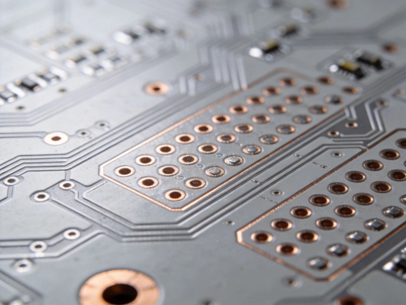
High-Density Interconnect boards represent a significant advancement in PCB technology. Unlike traditional PCBs, HDI boards feature finer lines and spaces, smaller vias, and higher connection pad density. This allows designers to pack more components into a smaller area without compromising performance.
The key characteristics of HDI boards include:
These features make HDI boards ideal for applications where space is at a premium but performance cannot be compromised. From smartphones to medical implants, HDI technology enables the miniaturization that modern electronics demand.
Surface Mount Technology assembly is the perfect companion for HDI board production. SMT allows components to be mounted directly onto the PCB surface, eliminating the need for through-hole leads that would consume valuable board real estate. This is especially critical for HDI applications where space optimization is paramount.
When customizing Smt Pcb Assembly for HDI boards, several factors come into play:
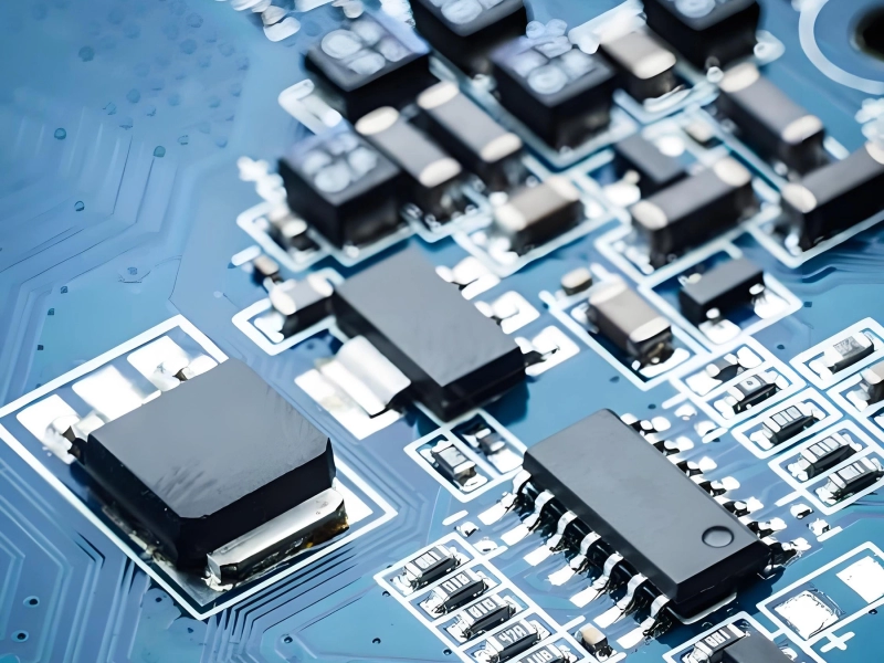
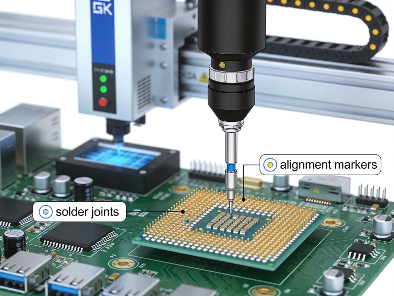
HDI boards often require placement of extremely small components, including chip-scale packages (CSP) and micro BGAs with pitches as fine as 0.3mm. Advanced pick-and-place equipment with high-resolution vision systems ensures accurate component positioning. Chinese manufacturers have invested heavily in state-of-the-art SMT equipment capable of handling these demanding requirements.
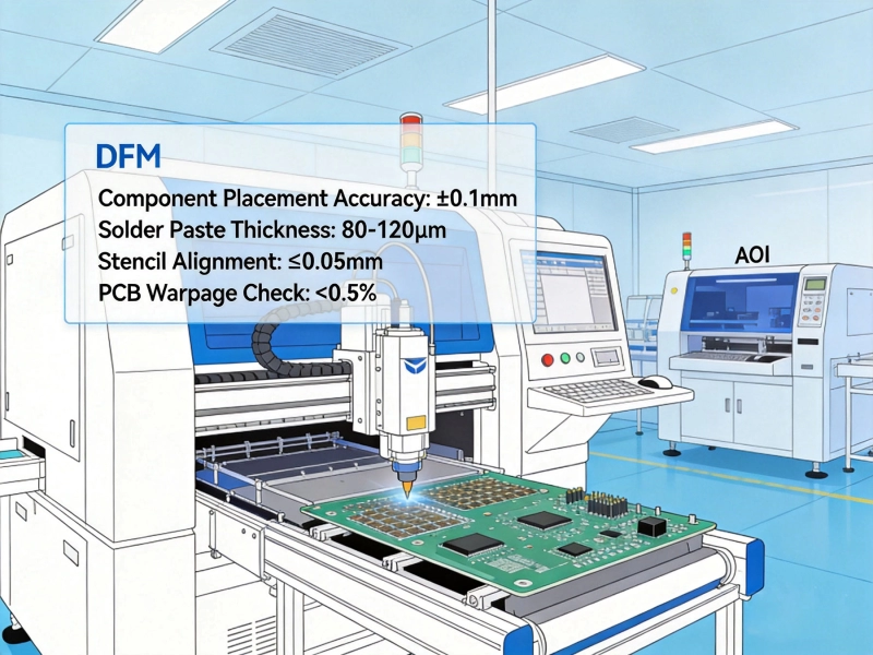
The fine pitch of HDI components demands precise solder paste printing. Laser-cut stencils with thicknesses as low as 80 microns are commonly used to achieve the necessary accuracy. Quality manufacturers in China employ Automated Optical Inspection (Aoi) after paste printing to catch defects before they become costly rework issues.
Proper Thermal Management during reflow is critical for HDI assemblies. The dense component placement can create thermal gradients that affect solder joint quality. Experienced Chinese SMT facilities develop customized reflow profiles that ensure uniform heating across the entire board, preventing tombstoning, voiding, and other defects.
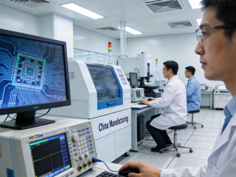
China has established itself as a global leader in Pcb Manufacturing and Smt Assembly, particularly for HDI applications. Here's why partnering with Chinese manufacturers makes sense for your HDI projects:
Chinese manufacturers offer competitive pricing due to economies of scale and established supply chains. However, cost savings don't mean quality sacrifices. Many facilities hold ISO 9001, ISO 13485 for medical devices, and IPC certifications ensuring consistent quality standards. The key is selecting manufacturers with proven track records in HDI production.
Leading Chinese PCB facilities have made substantial investments in HDI-specific equipment. This includes laser direct imaging systems for fine-line patterning, sequential lamination presses for build-up construction, and advanced SMT lines with 01005 component capability. These investments enable production of cutting-edge HDI designs that would be difficult or impossible with older equipment.
Speed to market is crucial in today's competitive electronics landscape. Chinese manufacturers excel at quick-turn prototyping, often delivering HDI samples within 3-5 days. Once designs are validated, the same facilities can scale to high-volume production seamlessly, eliminating the delays and quality risks associated with switching manufacturers between prototype and production phases.
Many Chinese PCB manufacturers provide end-to-end services including Design For Manufacturability (Dfm) review, component sourcing, assembly, testing, and logistics. This integrated approach reduces coordination overhead and potential communication issues that can arise when working with multiple vendors.
Successful HDI board production requires careful attention to design details. Working closely with your Chinese manufacturing partner during the design phase can prevent costly issues later. Consider these critical factors:
HDI boards utilize various via structures including microvias, blind vias, buried vias, and via-in-pad designs. Each type serves different purposes and has specific manufacturability requirements. Via-in-pad designs, for example, allow components to be placed directly over vias but require careful planning for plating and filling to prevent solder joint defects.
When designing for Smt Assembly in China, communicate your via strategy clearly. Provide stackup information and via construction details to ensure the manufacturer can execute your design correctly. Many HDI failures trace back to inadequate via design or manufacturing inconsistencies.
Choose components that align with HDI capabilities and your assembler's equipment. While 01005 components are possible, they require specialized handling and increase assembly costs. Consider whether the space savings justify the added complexity and risk.
Maintain adequate spacing between components to allow for rework and inspection. The temptation to maximize density must be balanced against manufacturability and yield considerations. Your Chinese manufacturing partner can provide Dfm feedback on component placement strategies.
HDI boards pack significant power dissipation into small volumes, making Thermal Management crucial. Work with your manufacturer to incorporate thermal vias, copper pours, and appropriate substrate materials. High-TG laminates and metal-core substrates are available options for thermally challenging applications.
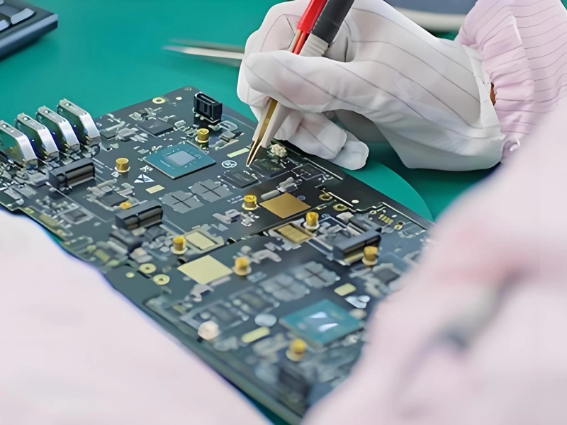
Quality Assurance is paramount for HDI assemblies where defects can be difficult to detect and expensive to repair. Reputable Chinese manufacturers implement comprehensive quality control measures:
Component and bare board inspection before assembly prevents problems downstream. For HDI boards, this includes verification of via integrity, surface finish quality, and dimensional accuracy. Advanced facilities use X-ray inspection to verify via filling and internal layer alignment.
Statistical process control (SPC) monitors critical parameters throughout the SMT process. Solder paste height, placement accuracy, and reflow temperatures are tracked continuously. Automatic alerts notify operators when parameters drift outside acceptable limits, enabling quick corrective action.
Automated Optical Inspection (Aoi) checks for component presence, polarity, and solder joint quality. X-ray inspection verifies hidden solder connections, particularly for BGA and QFN components common in HDI designs. Functional testing validates electrical performance according to customer specifications.
HDI SMT assembly in China presents unique challenges, but experienced manufacturers have developed effective solutions:
The dense routing and multiple via transitions in HDI boards can create Signal Integrity challenges. Work with manufacturers who have RF engineering expertise and can perform Signal Integrity simulations. Controlled Impedance stackups and appropriate via structures mitigate these issues.
The global component shortage has affected HDI assemblies disproportionately due to their specialized component requirements. Chinese manufacturers often have established relationships with multiple suppliers and can provide component sourcing assistance. Consider allowing approved substitutions during the design phase to maintain flexibility.
While language differences can create challenges, most established Chinese manufacturers have English-speaking engineering teams. Provide clear, detailed specifications and ask questions when clarification is needed. Regular video calls and shared project management tools improve communication effectiveness.
Not all PCB manufacturers have the capabilities and experience for HDI SMT assembly. When evaluating potential partners, consider:
The HDI landscape continues to evolve, driven by demands for even greater density and performance. Several trends are shaping the future of HDI SMT assembly in China:
Any-layer HDI technology enables microvias to connect any two layers in a board, providing unprecedented routing flexibility. While more expensive than traditional HDI structures, any-layer HDI is becoming necessary for the most demanding applications.
Embedded component technology places passive and active components within the board substrate itself, further reducing surface area requirements. Chinese manufacturers are investing in this technology to meet future miniaturization demands.
Advanced packaging technologies including fan-out wafer-level packaging (FOWLP) and 2.5D/3D IC integration are extending HDI concepts to new levels. These technologies require close collaboration between design teams and manufacturing partners.
Customizing Smt Pcb Assembly in China for HDI boards offers a compelling combination of technical capability, cost efficiency, and manufacturing scalability. Success requires careful attention to design details, clear communication with manufacturing partners, and rigorous quality control throughout the production process.
By understanding HDI technology principles, SMT assembly requirements, and the specific advantages that Chinese manufacturers offer, you can successfully navigate the complexities of HDI production and bring competitive products to market faster.
The key is partnering with experienced manufacturers who have demonstrated HDI capabilities and a commitment to quality. With the right partner, China's Pcb Manufacturing industry provides the resources and expertise needed to realize even the most demanding HDI designs.
HDI boards typically feature line and space dimensions of 3 mil or less, with microvia diameters under 0.15mm. Advanced HDI processes can achieve even finer features, down to 2 mil lines and spaces, though this increases manufacturing complexity and cost.
Prototype HDI boards typically require 3-5 days for fabrication plus 1-2 days for SMT assembly. Production quantities depend on volume and complexity but generally range from 1-3 weeks. Rush services are available from many manufacturers for time-critical projects.
Look for ISO 9001 for quality management, ISO 14001 for environmental management, and Ipc Standards compliance. For specific industries, additional certifications like ISO 13485 for medical devices, IATF 16949 for automotive, or AS9100 for aerospace may be required.
While HDI boards can accommodate through-hole components, they are generally avoided due to space constraints. Mixed-technology assemblies are possible but complicate the manufacturing process. Most HDI designs use all surface-mount components for optimal density.
HDI boards typically cost 2-4 times more than standard PCBs due to additional manufacturing steps, specialized materials, and tighter tolerances. However, the total system cost may be lower due to reduced board size and simplified assembly in the final product.
Request detailed quality documentation including inspection reports, test results, and process control data. Consider third-party inspection for critical applications. Establish clear acceptance criteria upfront and maintain open communication throughout the production process.
Contact experienced Chinese HDI manufacturers today to discuss your requirements. With proper planning and the right manufacturing partner, you can leverage HDI technology to create smaller, more powerful electronic products that meet today's demanding market requirements.
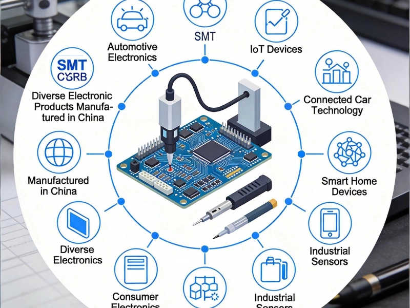
Top Applications of SMT PCB Assembly in China From Automotive to IoTMay/29/2026
How to Get Quick-turn SMT PCB Assembly in Just 24 Hours from ChinaMay/29/2026
How a Top High Frequency PCB Manufacturer Ensures Signal IntegrityJune/02/2026
Essential DFM Guidelines for SMT PCB Assembly in ChinaJune/04/2026
How to Design the Perfect Land Pattern for SMT Components in Chinese FactoriesJune/18/2026
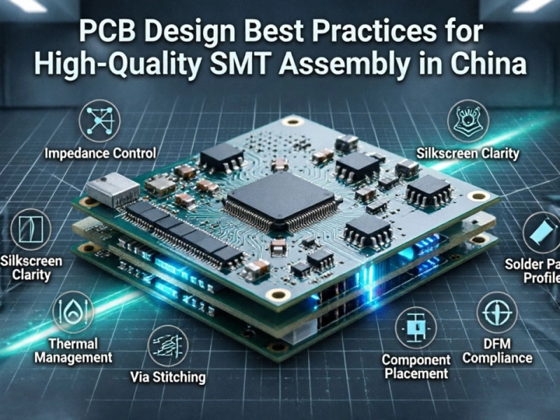
PCB Design Best Practices for High-Quality SMT Assembly in ChinaJune/05/2026
Overcoming BGA Challenges in a Complex SMT PCB Assembly China ProjectJune/09/2026
Overcoming BGA Challenges in a Complex SMT PCB Assembly China ProjectMay/29/2026