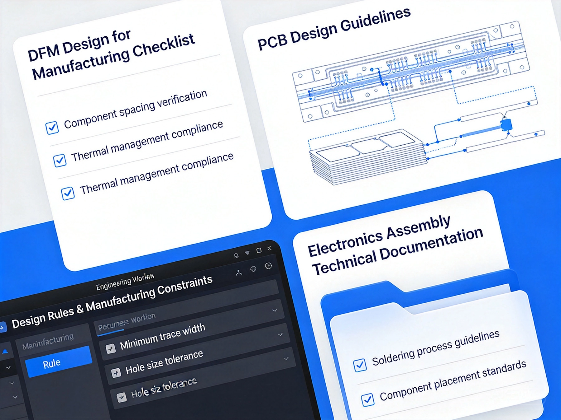
Designing PCBs for manufacturability is the difference between designs that work smoothly in production and designs that cause endless headaches. In China's competitive Smt Assembly environment, following proper Dfm (Design for Manufacturing) guidelines prevents costly rework, reduces production delays, and improves final product quality. This 2026 checklist covers the essential guidelines that top Chinese PCB assembly facilities expect from designers who want smooth production.
We've developed this guide based on real-world experience working with Chinese PCB manufacturers, current industry standards, and common failure modes we see repeatedly. Whether you're designing for a new product or optimizing an existing design, this checklist helps you catch Dfm issues before they reach the factory floor. Following these guidelines doesn't guarantee perfect production, but it dramatically reduces the likelihood of common assembly problems.
Before diving into specific guidelines, let's be clear why DFM matters. Poor DFM creates real, measurable problems in production. Understanding the impact helps justify the time spent on DFM review.
Common DFM failure consequences:
Most DFM problems are preventable with upfront design attention. Catching issues during design review might take hours. Fixing the same issues after fabrication and assembly can take weeks and cost much more.
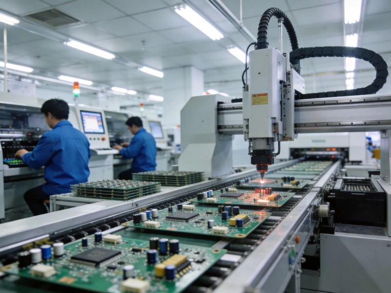
Chinese PCB assembly facilities operate at high volume with tight cost pressures. They've optimized their processes for efficiency, and designs that don't match their capabilities create friction. Understanding the Chinese manufacturing context helps you design for their capabilities rather than against them.
Chinese assembly characteristics:
Top Chinese facilities can handle complex designs, but they appreciate designs that respect their standard processes. When you design within their capabilities, you get better results at lower cost with fewer headaches.
Your PCB layer stack-up fundamentally affects both fabrication and assembly quality. Good stack-up design provides the foundation for reliable assembly.
Stack-up DFM principles:
Common stack-up mistakes to avoid:
Work with your PCB fabricator on stack-up design. They can recommend standard stack-ups that optimize for both fabrication and assembly performance.
Trace width and spacing must balance electrical requirements with fabrication capability. Traces too close together cause shorts during assembly. Traces too narrow cause fabrication yield problems.
Trace width guidelines:
Trace spacing guidelines:
For very dense designs, consider whether you need to use more layers to reduce density. Sometimes adding a layer costs less than fighting tight spacing constraints.
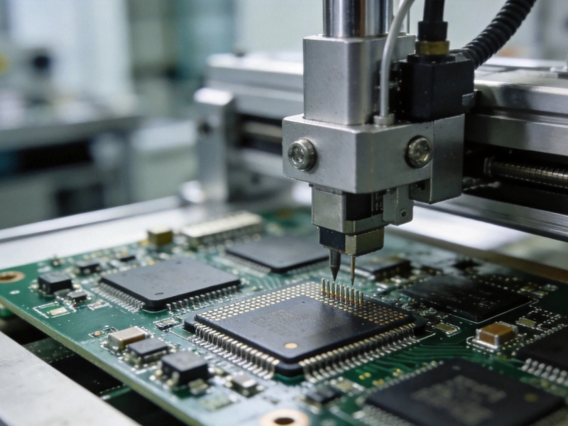
Vias create necessary interconnections between layers, but they also create manufacturing challenges. Good via design balances electrical needs with fabrication practicality.
Via size guidelines:
Via placement considerations:
For high-density designs requiring many vias, consider blind and buried vias to save space. These vias cost more but can enable designs that wouldn't be possible with through-vias only.
Solder mask protects copper traces and defines where solder should form. Silkscreen provides component markings and assembly guidance. Both must be designed for manufacturability.
Solder mask guidelines:
Silkscreen guidelines:
Minimize silkscreen content to essential information - component designators, polarity marks, and critical assembly information. Excessive silkscreen creates confusion during assembly.
Component spacing affects manufacturability significantly. Components too close together cause assembly problems, but excessive spacing wastes board space. Finding the right balance is key.
Component spacing guidelines:
Special spacing considerations:
For automated assembly, component spacing affects machine operation. Components too close together can cause pick-and-place machine collisions or interfere with reflow heating.
Component orientation affects manufacturability and inspection. Consistent orientation makes assembly more efficient and inspection easier.
Orientation guidelines:
Benefits of consistent orientation:
Choose component sizes that balance your design requirements with manufacturability considerations. Smaller isn't always better when it affects assembly reliability.
Component size guidelines:
When to consider smaller components:
Confirm with your assembly partner what component sizes they handle reliably. Don't specify component sizes smaller than their capabilities unless absolutely necessary.
PCB pads must be designed to match component leads properly. Incorrect pad sizing causes soldering defects and component placement problems.
Pad sizing principles:
Common pad design mistakes:
Use standard footprints from your EDA tool libraries or component manufacturer recommendations. Custom footprints should follow established guidelines rather than being created from scratch.
Thermal relief pads provide connection to large copper areas while allowing soldering heat to reach the pad effectively. Poor thermal relief design creates soldering problems.
Thermal relief guidelines:
When thermal relief is necessary:
Not all pads need thermal relief. Direct connections without thermal relief provide better electrical performance when soldering isn't a concern.
Fiducial marks provide reference points for Machine Vision alignment during assembly. Proper fiducial design improves placement accuracy and reduces assembly errors.
Fiducial guidelines:
Fiducial placement:
Fiducials are especially important for high-density boards with fine-pitch components. For simpler boards, fiducials might not be necessary, but they rarely hurt.
Solder paste application happens before component placement and affects assembly quality. Your design should facilitate proper solder paste deposition.
Solder paste considerations:
Paste deposition issues to avoid:
Work with your assembly partner on stencil design. They have experience with what works for specific components and can recommend appropriate stencil configurations.
Your board and component selection affects the Reflow Soldering process. Understanding these effects helps you design for successful reflow.
Reflow-related design considerations:
Temperature-sensitive components:
Most modern components can handle standard reflow profiles, but some have temperature limitations. Be aware of these limitations during component selection.
For designs requiring through-hole assembly after SMT, wave soldering considerations affect component placement and board layout.
Wave soldering DFM considerations:
Wave soldering fixture design:
Many modern designs avoid wave soldering by using through-hole connectors only and keeping everything else SMT. When wave soldering is necessary, follow these guidelines to ensure success.
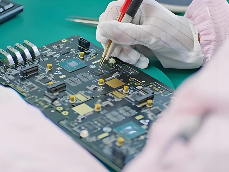
Test points enable in-circuit testing and functional testing. Well-designed test points improve testability and reduce test development time.
Test point guidelines:
Test point placement:
Test points add cost through increased board area and test fixture complexity. Balance testability needs against cost considerations. For high-volume production, better testability typically pays for itself through reduced test time and improved quality.
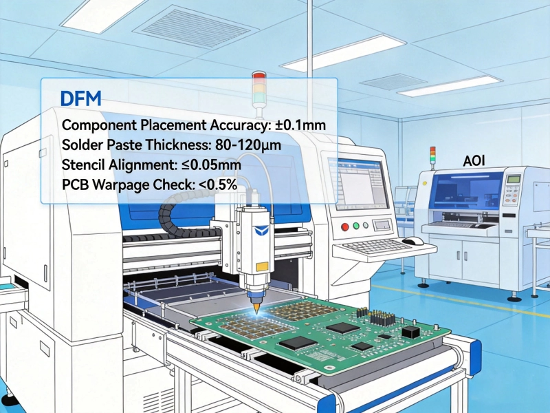
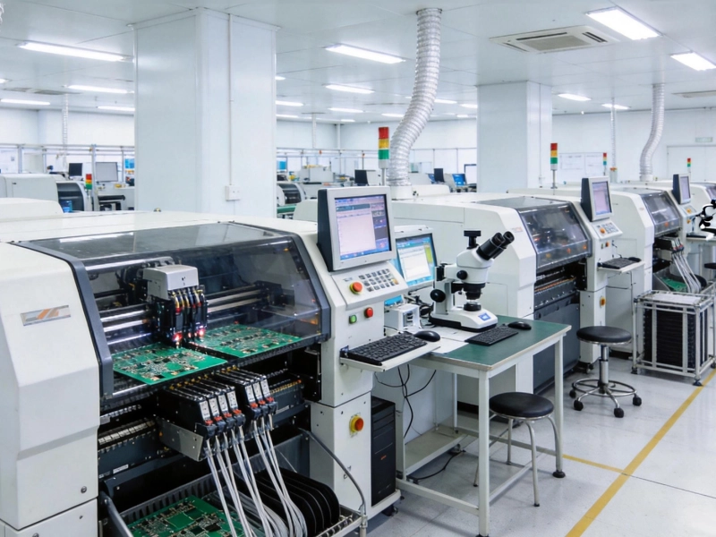
Your design should facilitate visual inspection and Automated Optical Inspection (Aoi). Good inspection design helps catch defects before boards progress too far in assembly.
Inspection-friendly design:
Aoi considerations:
AOI is increasingly common in Chinese assembly facilities. Designing with AOI in mind improves inspection effectiveness and reduces false defect calls.
Complete, accurate design files are essential for smooth manufacturing. Incomplete or ambiguous files cause delays and mistakes.
Essential design files:
File quality considerations:
Chinese assembly facilities work with many customers and understand that design file quality varies. Providing complete, accurate files demonstrates professionalism and helps avoid problems.
Clear assembly notes and specifications prevent misunderstandings and ensure your requirements are met.
Essential assembly documentation:
Common communication gaps:
Good communication starts with good documentation. Taking time to document requirements clearly saves time later by preventing problems and clarifications.
Use this checklist before sending your design to assembly. Reviewing these items catches common DFM problems before they cause production issues.
Pcb Design Checklist:
Component Placement Checklist:
Pad Design Checklist:
Assembly Considerations Checklist:
Documentation Checklist:
Before production starts, engage with your assembly partner for design review. Their input can catch DFM issues you might have missed and suggest optimizations based on their capabilities.
Discussion topics for pre-production review:
A good assembly partner will provide constructive feedback during review. Take their suggestions seriously - they have experience with what works and doesn't work in their production environment.
After initial production, perform thorough first article inspection to confirm production meets your requirements before full production begins.
First article inspection items:
First article inspection catches problems early. Address any issues before committing to full production. This proactive approach prevents producing large quantities of defective boards.
After reviewing countless designs, certain Dfm Mistakes appear repeatedly. Avoiding these common errors prevents many problems.
Most common Dfm Mistakes:
Design practices to avoid:
Many DFM mistakes result from rushing design or not thinking through assembly consequences. Taking time for DFM review prevents these mistakes.
Good DFM practices distinguish designs that assemble smoothly from designs that create endless problems. This 2026 checklist provides the essential guidelines that Chinese Smt Assembly facilities expect from designers. Following these guidelines doesn't guarantee perfection, but it dramatically improves your chances of successful production.
The key insight is that manufacturability isn't an afterthought - it should inform design decisions from the beginning. Component selection, layout, and even design tool choices should consider manufacturability alongside functional requirements. When manufacturability is part of the design process rather than an add-on review, you naturally avoid many common DFM problems.
Chinese assembly facilities have optimized their processes for efficiency and quality. Designs that work within their processes benefit from this optimization. Designs that fight standard processes create friction that costs money and time. Understanding this dynamic and designing accordingly gives you better results.
DFM review isn't wasted time - it's an investment in production success. The hours spent on DFM review save days or weeks of production problems later. For anyone designing PCBs for Chinese SMT assembly, this checklist provides the foundation for designs that assemble successfully and reliably.
Q: How do I know if my design is ready for manufacturing?
A>Use the checklists provided in this article as a starting point. Then engage with your assembly partner for pre-production review. Their specific feedback based on their capabilities provides the definitive assessment. If they identify no major concerns, your design is ready for manufacturing.
Q: Should I design for specific assembly equipment or general capabilities?
A>Design for general capabilities unless you have a specific reason to target particular equipment. General capabilities provide flexibility if you need to switch assembly partners. Targeting specific equipment makes sense for very high volume where equipment optimization matters.
Q: What if my design violates some Dfm Guidelines?
A>Some violations might be acceptable depending on their impact. Work with your assembly partner to assess which violations matter and which can be accommodated. Some violations increase cost or risk but might still be acceptable. Others might make production impossible or impractical.
Q: How often do DFM requirements change?
A>Core DFM principles remain stable, but capabilities evolve as equipment improves. Component miniaturization continues, enabling smaller features. Process improvements reduce tolerance limitations. The guidelines in this article reflect current 2026 capabilities but stay updated with assembly partner developments.
Q: Can I save board space by ignoring some Dfm Guidelines?
A>You might reduce board size temporarily, but you'll likely pay more through higher assembly costs, lower yields, or rework. The space savings often don't justify the manufacturing problems. Better solutions include using more layers, different components, or redesign for better space efficiency without violating DFM guidelines.
Top 10 DFM Mistakes to Avoid Before Sending Files to China for SMT AssemblyJuly/14/2026

Optimizing PCB Design for Chinese SMT ManufacturersJuly/02/2026
How to Reduce SMT PCB Assembly Costs in China with Early DFM AnalysisJune/17/2026
Essential DFM Guidelines for SMT PCB Assembly in ChinaJune/04/2026
Customizing SMT PCB Assembly China Applications for High-Density Interconnect (HDI) BoardsJune/22/2026
Overcoming BGA Challenges in a Complex SMT PCB Assembly China ProjectMay/29/2026
How to Get Quick-turn SMT PCB Assembly in Just 24 Hours from ChinaJune/12/2026
The Complete Process WalkthroughMay/29/2026