Open Nav

Industrial equipment runs on power. Motor drives, power converters, welding equipment, and battery management systems all demand PCBs that can handle currents far exceeding what Consumer Electronics require. In China, manufacturers have developed specialized capabilities for heavy copper PCB fabrication and high-power component assembly that serve the global industrial market. Understanding how these boards are made and what challenges they present helps you design more reliably and work more effectively with Chinese assembly partners.
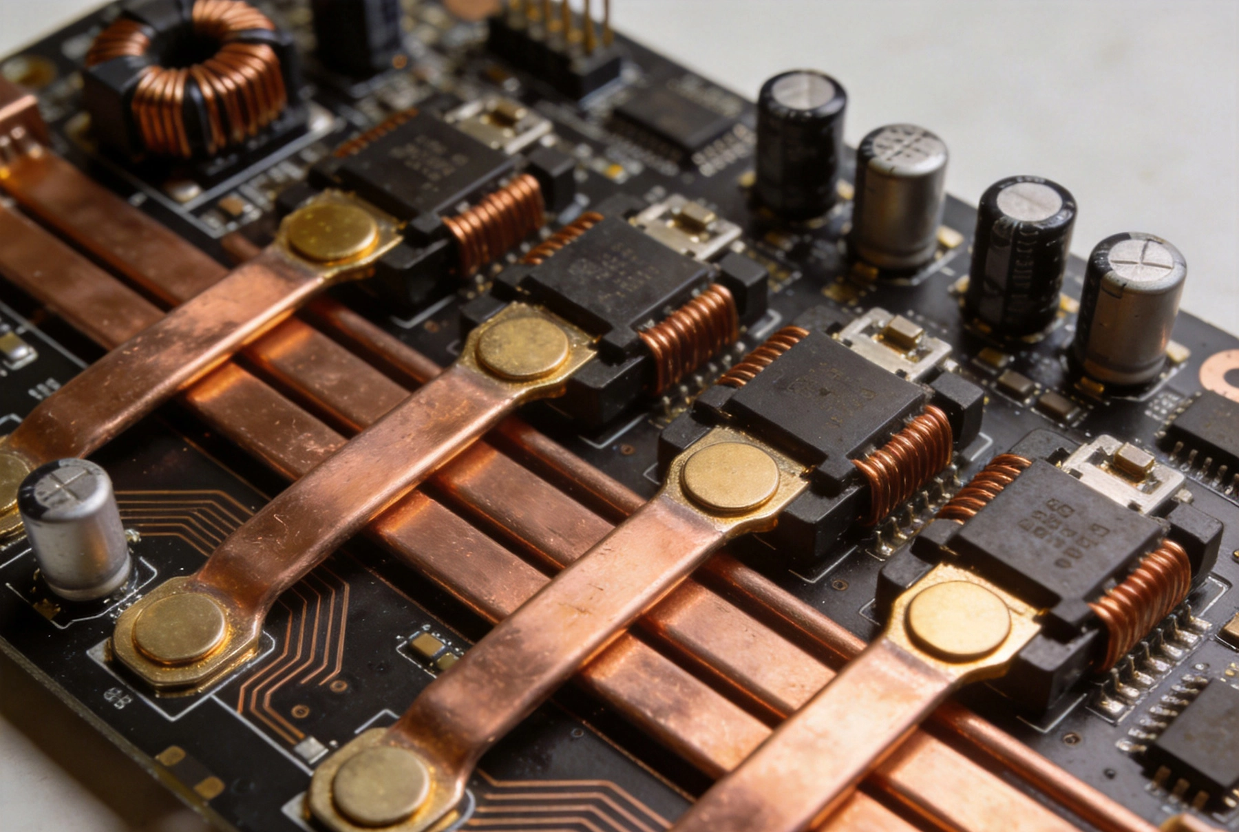
Standard PCB copper weight is 1 oz per square foot (approximately 35 microns thickness). Heavy copper is typically defined as 2 oz or more, with some designs using 3 oz, 4 oz, or even 6 oz copper for extreme current applications. At 4 oz copper, the trace thickness is over 140 microns—four times standard copper—which dramatically increases current-carrying capacity and thermal conductivity.
The jump from standard to heavy copper is not just about thicker metal. Heavy copper boards require different processing at every stage: imaging, etching, plating, and soldermask. A fabricator experienced with standard 1 oz boards may struggle with 4 oz material without specialized equipment and process controls. China's Industrial Pcb manufacturers have invested in these capabilities specifically to serve the global market for power electronics.
Heavy copper traces can carry substantially more current than standard traces, but the relationship is not simply linear. Wider traces provide more current capacity, but the thermal benefit of heavy copper also depends on how effectively heat can spread from the trace into the surrounding copper plane and ultimately to the board surface where it dissipates.
Thermal relief patterns connect heavy copper planes to component pads. These spoke-like connections restrict heat flow during soldering, ensuring that the pad reaches reflow temperature without the large copper plane acting as a heat sink that prevents solder melting. The number and width of thermal relief spokes must be balanced—too few spokes create high thermal resistance, while too many reduce the mechanical robustness of the connection.
For components that carry the highest currents—IGBT modules, MOSFETs in large packages, bus bars—direct copper attachment (DCA) or press-fit terminals may be more appropriate than standard SMT. These approaches provide lower thermal resistance and higher current capacity than soldered connections, but they require specialized assembly processes and are typically handled by dedicated power Electronics Assembly houses.
Heavy copper boards often require high-Tg materials to handle the thermal loads generated by high currents. Standard FR-4 with Tg of 130–140°C may be insufficient for boards where internal temperatures can approach 100°C during operation. High-Tg FR-4 (Tg above 150°C) or polyimide provides the thermal margin needed for reliable long-term operation.
Metal-backed substrates are common for very high-power applications. Aluminum core boards or copper core boards conduct heat away from power components more effectively than FR-4, allowing higher power density in the same footprint. The thermal interface between the component and the metal backing is critical—thermal pads, thermal interface material, and mechanical mounting pressure all affect thermal performance.
For multilayer heavy copper boards, the distribution of copper across layers matters for balanced construction. Uneven copper distribution causes warpage during lamination and reflow. Use copper fill on all layers, even if those layers are primarily ground or power planes, to maintain balanced construction.
Heavy copper assembly presents challenges that standard SMT processes are not designed to handle. The most significant is solder paste deposition. Heavy copper planes act as heat sinks that draw heat away from the joint area during reflow, preventing proper solder melting if the thermal relief design is inadequate or the Reflow Profile is not adjusted.
Chinese SMT assemblers experienced with power electronics modify their reflow profiles for heavy copper boards. The soak zone is extended to allow the board to reach thermal equilibrium before the reflow spike. The peak temperature may be held slightly higher or longer to ensure complete solder reflow despite the thermal mass of heavy copper planes. The cooling rate is controlled to minimize thermal shock to components and plated-through holes.
Component Placement accuracy matters more for power components that have large thermal pads. Misalignment of a 10 mm by 10 mm power pad creates a larger percentage void than the same misalignment on a 2 mm by 2 mm logic IC pad. Modern SMT placers with vision systems handle this well, but the placement program must be optimized for the larger components.
Current must flow between layers in a multilayer board, which means vias carry current as well as traces. A standard 0.3 mm diameter via can carry approximately 1–2 amperes safely. For higher currents, you need more vias, larger vias, or vias filled with solder or conductive paste.
Slot vias—elongated holes that follow the trace direction—provide more cross-sectional area than round vias of the same width. A 0.3 mm wide slot via has roughly three times the current capacity of a 0.3 mm round via. Slot vias are common in heavy copper designs and require careful design rules because they have different thermal relief characteristics than round vias.
Via-in-pad with solder fill is used for the most demanding thermal and current applications. The solder-filled via conducts heat from the component pad to internal planes and provides a redundant current path. This approach requires additional processing—via filling, planarization, and sometimes a second plating cycle—but achieves the lowest thermal resistance for power component attachment.
High-power assemblies require testing beyond standard ICT and Aoi. Thermal imaging during operation identifies hot spots that indicate current crowding or poor thermal interface. A board that passes electrical testing at room temperature may develop open joints or high-resistance connections under thermal stress.
Temperature cycling testing is particularly important for power assemblies. The combination of self-heating from current flow and ambient temperature variations creates thermal stress that can crack solder joints over time. Boards should be tested to the temperature range they will experience in the actual application, with the components powered to their expected operating levels.
Destructive physical analysis of early production samples provides confidence in the assembly process. Cross-sectioning a representative sample board reveals the quality of solder joints, via fill, and plating thickness. For safety-critical applications like automotive or medical power supplies, this testing is required for qualification.
China has become the primary source for heavy copper PCB fabrication globally. The equipment investments required for heavy copper—specialty etchers, plating tanks capable of thick copper deposition, and controlled lamination processes—are substantial, and Chinese manufacturers have made these investments to serve industrial customers worldwide.
When specifying heavy copper work to a Chinese manufacturer, provide clear documentation of current requirements per trace, maximum allowable temperature rise, and thermal interface expectations. The more specific you are about what the board needs to do, the better they can optimize the Design For Manufacturing and performance.
Request qualification samples before full production. A small run of 5–10 boards allows you to test the assembly in your application, verify thermal performance, and identify any issues before committing to high-volume production. Most Chinese manufacturers offer prototype runs at reasonable prices specifically for this purpose.
Quality expectations should be clearly communicated. For industrial applications, Ipc Class 3 acceptance criteria are typical, but you may have additional requirements around specific defects—void content in plated through-holes, minimum annular ring width for heavy copper vias, or thermal cycling test results. Document these requirements in your purchase agreement.
Heavy copper boards cost more than standard copper weight boards. The incremental cost comes from specialized plating processes, longer etch times, and higher reject rates when process control is not optimal. However, heavy copper often replaces a more complex solution—such as discrete bus bars, additional connector hardware, or multiple parallel standard boards—so the total system cost may be lower.
Volume affects heavy copper pricing significantly. At low volumes, the setup costs dominate and per-board pricing is high. At high volumes, setup costs amortize across many units and the per-board cost approaches that of standard boards. If your product has a long production life, the investment in heavy copper fabrication pays back over time through reduced system complexity and assembly cost.
The assembly cost for heavy copper boards is also higher. Extended reflow profiles, specialized thermal relief handling, and more stringent testing all add to the per-board cost. Factor these costs into your total cost analysis when comparing heavy copper against alternative high-current distribution approaches.
Heavy copper PCBs are essential for industrial power applications, and Chinese manufacturers have the capabilities and experience to produce them reliably. Designing for manufacturability, communicating requirements clearly, and qualifying the process before high-volume production are the keys to a successful heavy copper project.
The Demands of Industrial SMT PCB Assembly in ChinaMay/29/2026
Why IPC Class 3 Standards Matter for Industrial SMT PCB Assembly in ChinaJune/28/2026

SMT PCB Assembly for Harsh Environments: Conformal Coating Solutions in ChinaJuly/18/2026

Ensuring Long-Term Supply Chain Stability for Industrial SMT Assembly in ChinaSeptember/03/2026
Why IPC Class 3 Standards Matter for Industrial SMT PCB Assembly in ChinaJuly/08/2026
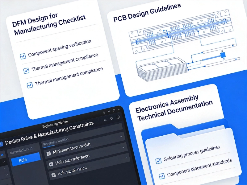
Essential DFM Guidelines for SMT PCB Assembly in ChinaMay/29/2026
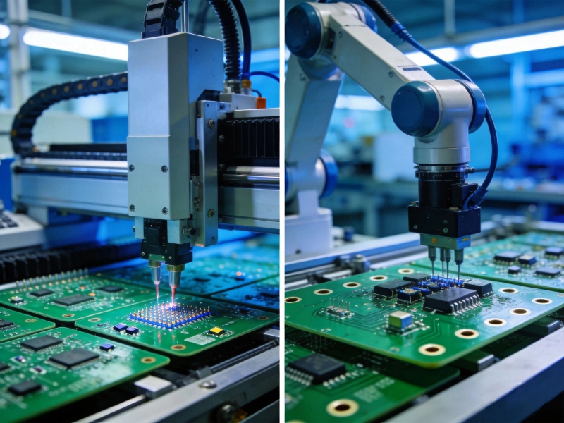
SMT vs THT PCB Assembly in China: Which Technology is Right for Your Project?June/08/2026
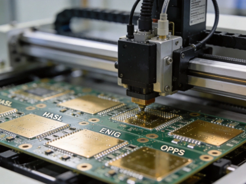
The Impact of PCB Surface Finish on SMT Assembly Soldering Quality in ChinaAugust/06/2026